- 您現(xiàn)在的位置:買(mǎi)賣(mài)IC網(wǎng) > PDF目錄98143 > ST16C654IQ64/TR (EXAR CORP) 4 CHANNEL(S), 1.5M bps, SERIAL COMM CONTROLLER, PQFP64 PDF資料下載
參數(shù)資料
| 型號(hào): | ST16C654IQ64/TR |
| 廠商: | EXAR CORP |
| 元件分類(lèi): | 微控制器/微處理器 |
| 英文描述: | 4 CHANNEL(S), 1.5M bps, SERIAL COMM CONTROLLER, PQFP64 |
| 封裝: | 10 X 10 MM, 1.40 MM HEIGHT, LQFP-64 |
| 文件頁(yè)數(shù): | 2/54頁(yè) |
| 文件大?。?/td> | 734K |
| 代理商: | ST16C654IQ64/TR |
第1頁(yè)當(dāng)前第2頁(yè)第3頁(yè)第4頁(yè)第5頁(yè)第6頁(yè)第7頁(yè)第8頁(yè)第9頁(yè)第10頁(yè)第11頁(yè)第12頁(yè)第13頁(yè)第14頁(yè)第15頁(yè)第16頁(yè)第17頁(yè)第18頁(yè)第19頁(yè)第20頁(yè)第21頁(yè)第22頁(yè)第23頁(yè)第24頁(yè)第25頁(yè)第26頁(yè)第27頁(yè)第28頁(yè)第29頁(yè)第30頁(yè)第31頁(yè)第32頁(yè)第33頁(yè)第34頁(yè)第35頁(yè)第36頁(yè)第37頁(yè)第38頁(yè)第39頁(yè)第40頁(yè)第41頁(yè)第42頁(yè)第43頁(yè)第44頁(yè)第45頁(yè)第46頁(yè)第47頁(yè)第48頁(yè)第49頁(yè)第50頁(yè)第51頁(yè)第52頁(yè)第53頁(yè)第54頁(yè)
xr
ST16C654/654D
REV. 5.0.2
2.97V TO 5.5V QUAD UART WITH 64-BYTE FIFO
7
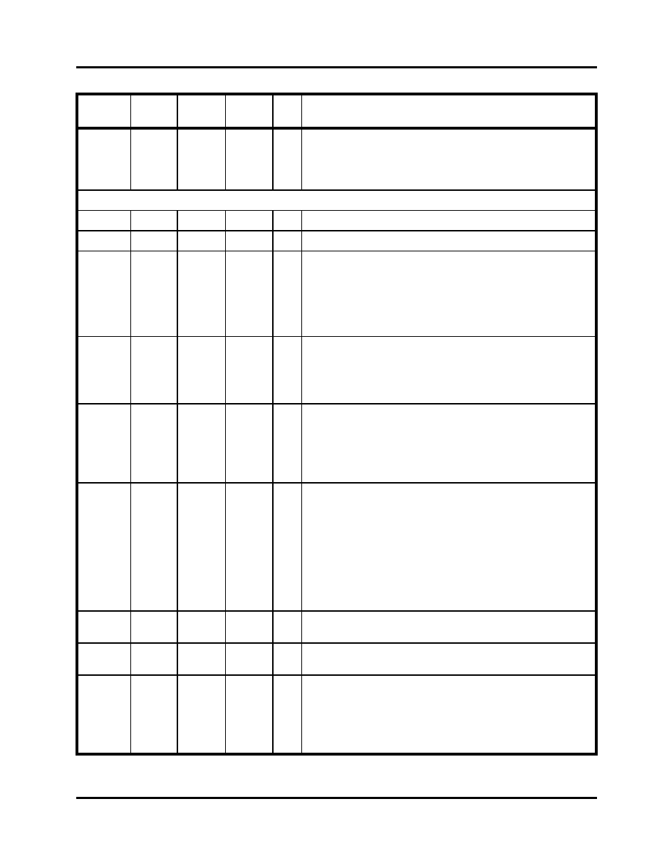
Pin type: I=Input, O=Output, I/O= Input/output, OD=Output Open Drain.
RIA#
RIB#
RIC#
RID#
63
19
30
50
8
28
42
62
98
33
48
84
I
UART channels A-D Ring-Indicator (active low) or general purpose
input. This input should be connected to VCC when not used. This
input has no effect on the UART.
ANCILLARY SIGNALS
XTAL1
25
35
40
I
Crystal or external clock input.
XTAL2
26
36
41
O
Crystal or buffered clock output.
16/68#
-
31
36
I
Intel or Motorola Bus Select (input with internal pull-up).
When 16/68# pin is at logic 1, 16 or Intel Mode, the device will oper-
ate in the Intel bus type of interface.
When 16/68# pin is at logic 0, 68 or Motorola mode, the device will
operate in the Motorola bus type of interface.
Motorola bus interface is not available on the 64 pin package.
CLKSEL
21
30
35
I
Baud-Rate-Generator Input Clock Prescaler Select for channels A-
D. This input is only sampled during power up or a reset. Connect to
VCC for divide by 1 (default) and GND for divide by 4. MCR[7] can
override the state of this pin following a reset or initialization. See
MCR bit-7 and Figure 6 in the Baud Rate Generator section.
CHCCLK
-
42
I
This input provides the clock for UART channel C. An external 16X
baud clock or the crystal oscillator’s output, XTAL2, must be con-
nected to this pin for normal operation. This input may also be used
with MIDI (Musical Instrument Digital Interface) applications when
an external MIDI clock is provided. This pin is only available in the
100-pin QFP package.
RESET
(RESET#)
27
37
43
I
When 16/68# pin is at logic 1 for Intel bus interface, this input becomes the
Reset pin (active high). In this case, a 40 ns minimum logic 1 pulse
on this pin will reset the internal registers and all outputs. The UART
transmitter output will be held at logic 1, the receiver input will be
ignored and outputs are reset during reset period (Table 16). When
16/68# pin is at a logic 0 for Motorola bus interface, this input
becomes Reset# pin (active low). This pin functions similarly, but
instead of a logic 1 pulse, a 40 ns minimum logic 0 pulse will reset
the internal registers and outputs.
Motorola bus interface is not available on the 64 pin package.
VCC
4, 35, 52
13, 47,
64
10, 61,
86
Pwr 2.97V to 5.5V power supply. The inputs are not 5V tolerant when
operating at 3.3V.
GND
14, 28,
45, 61
6, 23, 40,
57
20, 46,
71, 96
Pwr Power supply common, ground.
N.C.
-
1- 4, 26-
28, 29,
30, 51-
55, 77,
78, 79,
80
No Connection. These pins are not used in either the Intel or Motor-
ola bus modes. These pins are open, but typically, should be con-
nected to GND for good design practice.
Pin Description
NAME
64-LQFP
PIN #
68-PLCC
PIN#
100-QFP
PIN #
TYPE
DESCRIPTION
相關(guān)PDF資料 |
PDF描述 |
|---|---|
| ST18931CR | 16-BIT, 50 MHz, OTHER DSP, CPGA121 |
| ST40RA150XH6 | 32-BIT, 150 MHz, RISC PROCESSOR, PBGA372 |
| ST40RA200XH6E | 32-BIT, 200 MHz, RISC PROCESSOR, PBGA372 |
| ST52510F3M6 | MICROCONTROLLER, PDSO20 |
| ST52E430B/D | 8-BIT, UVPROM, 20 MHz, MICROCONTROLLER, CDIP32 |
相關(guān)代理商/技術(shù)參數(shù) |
參數(shù)描述 |
|---|---|
| ST16C654IQ64TR-F | 制造商:Exar Corporation 功能描述:UART 4-CH 64Byte FIFO 3.3V/5V 64-Pin LQFP T/R 制造商:Exar Corporation 功能描述:ST16C654IQ64TR-F |
| ST16CF54 | 制造商:STMICROELECTRONICS 制造商全稱:STMicroelectronics 功能描述:Smartcard MCU With 4 KBytes EEPROM 512 Bits Modular Arithmetic Processor |
| ST16CQ32245TBR | 功能描述:開(kāi)關(guān) IC - 各種 Advanced Logic Signal Switch RoHS:否 制造商:Fairchild Semiconductor 開(kāi)啟電阻(最大值): 電源電壓-最大:4.4 V 電源電壓-最小:2.5 V 最大工作溫度:+ 85 C 最小工作溫度:- 40 C 封裝 / 箱體:WLCSP-9 封裝:Reel |
| ST16DD00 | 功能描述:撥動(dòng)開(kāi)關(guān) TOGGLE RoHS:否 制造商:C&K Components 觸點(diǎn)形式:DPDT 開(kāi)關(guān)功能:ON - ON - ON 電流額定值: 電壓額定值 AC:20 V 電壓額定值 DC:20 V 功率額定值:0.4 VA 端接類(lèi)型:V-Bracket 安裝風(fēng)格: 端子密封:Epoxy 觸點(diǎn)電鍍:Gold 照明:Not Illuminated |
| ST16FJ | 制造商:Panasonic Electric Works 功能描述: |
發(fā)布緊急采購(gòu),3分鐘左右您將得到回復(fù)。