- 您現(xiàn)在的位置:買賣IC網(wǎng) > PDF目錄383836 > ST16C1451CQ48 (STARTECH SEMICONDUCTOR INC) 2.97V TO 5.5V UART PDF資料下載
參數(shù)資料
| 型號(hào): | ST16C1451CQ48 |
| 廠商: | STARTECH SEMICONDUCTOR INC |
| 元件分類: | 微控制器/微處理器 |
| 英文描述: | 2.97V TO 5.5V UART |
| 中文描述: | 1 CHANNEL(S), 448K bps, SERIAL COMM CONTROLLER, PQFP48 |
| 文件頁(yè)數(shù): | 7/32頁(yè) |
| 文件大小: | 355K |
| 代理商: | ST16C1451CQ48 |
第1頁(yè)第2頁(yè)第3頁(yè)第4頁(yè)第5頁(yè)第6頁(yè)當(dāng)前第7頁(yè)第8頁(yè)第9頁(yè)第10頁(yè)第11頁(yè)第12頁(yè)第13頁(yè)第14頁(yè)第15頁(yè)第16頁(yè)第17頁(yè)第18頁(yè)第19頁(yè)第20頁(yè)第21頁(yè)第22頁(yè)第23頁(yè)第24頁(yè)第25頁(yè)第26頁(yè)第27頁(yè)第28頁(yè)第29頁(yè)第30頁(yè)第31頁(yè)第32頁(yè)
á
REV. 4.2.0
ST16C1450/51
2.97V TO 5.5V UART
7
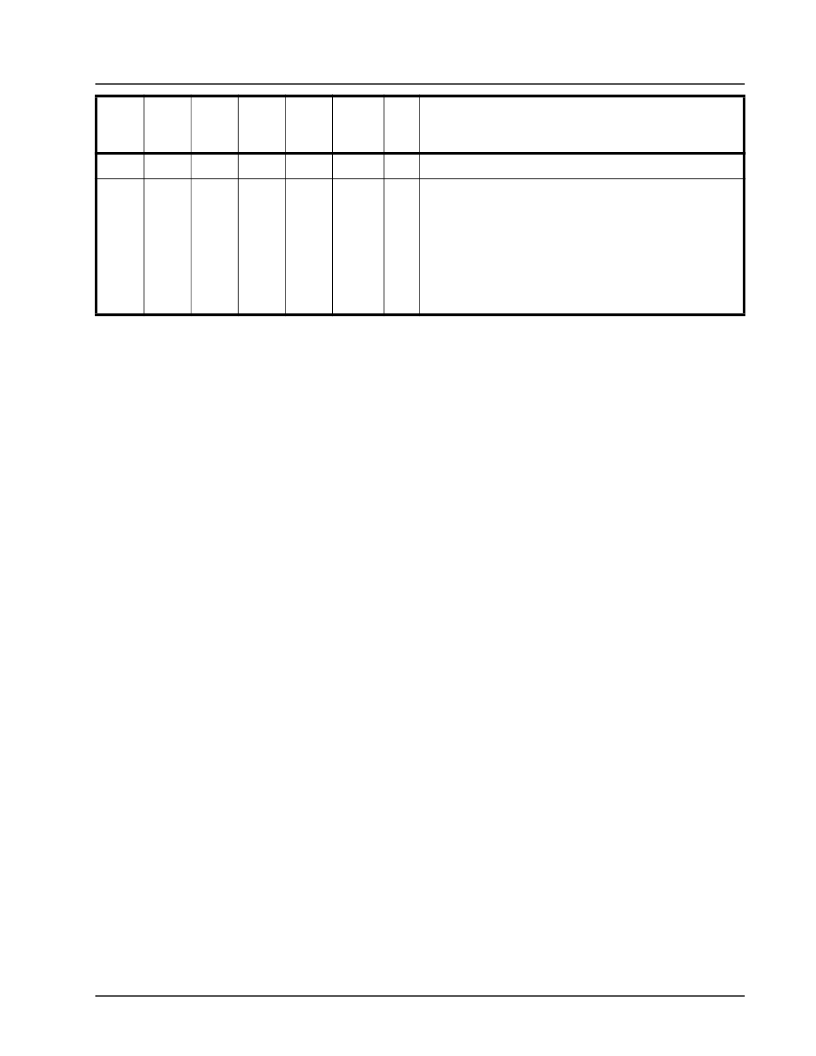
Pin type: I=Input, O=Output, I/O= Input/output, OD=Output Open Drain.
1.0
PRODUCT DESCRIPTION
The ST16C145X provides serial asynchronous receive data synchronization, parallel-to-serial and serial-to-
parallel data conversions for both the transmitter and receiver sections. These functions are necessary for
converting the serial data stream into parallel data that is required in digital data systems. Synchronization for
the serial data stream is accomplished by adding start and stops bits to the transmit data to form a data
character (character orientated protocol). Data integrity is ensured by attaching a parity bit to the data
character. The parity bit is checked by the receiver for any transmission bit errors. The 145X is capable of
operation up to 1.5 Mbps with a 24 MHz crystal or external clock input with a 16X sampling clock (at VCC =
5.0V). With a crystal of 14.7456 MHz and through a software option, the user can select data rates up to 921.6
Kbps.
2.0
FUNCTIONAL DESCRIPTIONS
2.1
The 145X has a set of enhanced registers for controlling, monitoring and data loading and unloading. These
registers function as data holding registers (THR/RHR), interrupt status and control registers (ISR/IER), a FIFO
control register (FCR), receive line status and control registers (LSR/LCR), modem status and control registers
(MSR/MCR), programmable data rate (clock) divisor registers (DLL/DLM), and a user accessible scractchpad
register (SPR). All the register functions are discussed in full detail later in
“Section 3.0, UART INTERNAL
REGISTERS” on page 13
.
Internal Registers
GND
15
14
15
14
19
Pwr
Power supply common ground.
N.C.
-
-
-
-
1, 2,
10-14,
18,
24-26,
29,
35-38,
42, 44,
48
-
Not connected.
N
AME
28-P
IN
PDIP
(1450)
28-P
IN
PDIP
(1451)
28-P
IN
PLCC
(1450)
28-P
IN
PLCC
(1451)
48-P
IN
TQFP
(145X)
T
YPE
D
ESCRIPTION
相關(guān)PDF資料 |
PDF描述 |
|---|---|
| ST16C1451IJ28 | 2.97V TO 5.5V UART |
| ST16C1451IP28 | 2.97V TO 5.5V UART |
| ST16C1451IQ48 | 2.97V TO 5.5V UART |
| ST16C1451 | 2.97V TO 5.5V UART |
| ST16C1550 | 2.97V TO 5.5V UART WITH 16-BYTE FIFO |
相關(guān)代理商/技術(shù)參數(shù) |
參數(shù)描述 |
|---|---|
| ST16C1451IJ28 | 制造商:EXAR 制造商全稱:EXAR 功能描述:2.97V TO 5.5V UART |
| ST16C1451IP28 | 制造商:EXAR 制造商全稱:EXAR 功能描述:2.97V TO 5.5V UART |
| ST16C1451IQ48 | 制造商:EXAR 制造商全稱:EXAR 功能描述:2.97V TO 5.5V UART |
| ST16C1550 | 制造商:EXAR 制造商全稱:EXAR 功能描述:2.97V TO 5.5V UART WITH 16-BYTE FIFO |
| ST16C1550_05 | 制造商:EXAR 制造商全稱:EXAR 功能描述:2.97V TO 5.5V UART WITH 16-BYTE FIFO |
發(fā)布緊急采購(gòu),3分鐘左右您將得到回復(fù)。