- 您現(xiàn)在的位置:買賣IC網(wǎng) > PDF目錄98139 > SNJ54LV123AW (TEXAS INSTRUMENTS INC) LV/LV-A/LVX/H SERIES, DUAL MONOSTABLE MULTIVIBRATOR, CDFP16 PDF資料下載
參數(shù)資料
| 型號: | SNJ54LV123AW |
| 廠商: | TEXAS INSTRUMENTS INC |
| 元件分類: | 諧振器 |
| 英文描述: | LV/LV-A/LVX/H SERIES, DUAL MONOSTABLE MULTIVIBRATOR, CDFP16 |
| 封裝: | CERAMIC, DFP-16 |
| 文件頁數(shù): | 1/28頁 |
| 文件大?。?/td> | 864K |
| 代理商: | SNJ54LV123AW |
當前第1頁第2頁第3頁第4頁第5頁第6頁第7頁第8頁第9頁第10頁第11頁第12頁第13頁第14頁第15頁第16頁第17頁第18頁第19頁第20頁第21頁第22頁第23頁第24頁第25頁第26頁第27頁第28頁
SN54LV123A, SN74LV123A
DUAL RETRIGGERABLE MONOSTABLE MULTIVIBRATORS
WITH SCHMITT-TRIGGER INPUTS
SCLS393O APRIL 1998 REVISED OCTOBER 2005
1
POST OFFICE BOX 655303
DALLAS, TEXAS 75265
D 2-V to 5.5-V V
CC Operation
D Max t
pd of 11 ns at 5 V
D Typical V
OLP (Output Ground Bounce)
<0.8 V at VCC = 3.3 V, TA = 25°C
D Typical V
OHV (Output VOH Undershoot)
>2.3 V at VCC = 3.3 V, TA = 25°C
D Support Mixed-Mode Voltage Operation on
All Ports
D Schmitt-Trigger Circuitry on A, B, and CLR
Inputs for Slow Input Transition Rates
D Edge Triggered From Active-High or
Active-Low Gated Logic Inputs
D I
off Supports Partial-Power-Down Mode
Operation
D Retriggerable for Very Long Output Pulses,
up to 100% Duty Cycle
D Overriding Clear Terminates Output Pulse
D Glitch-Free Power-Up Reset on Outputs
D Latch-Up Performance Exceeds 100 mA Per
JESD 78, Class II
D ESD Protection Exceeds JESD 22
2000-V Human-Body Model (A114-A)
200-V Machine Model (A115-A)
1000-V Charged-Device Model (C101)
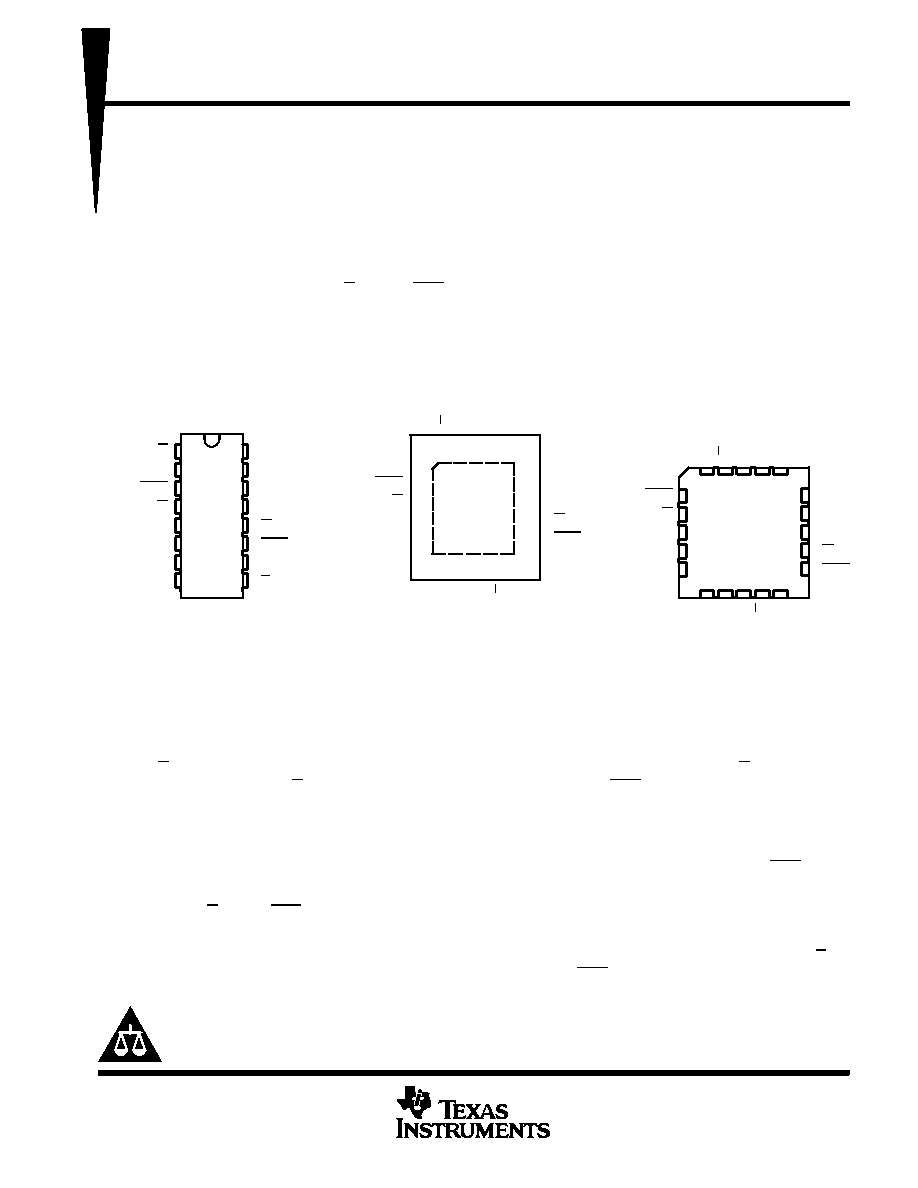
SN54LV123A ...J OR W PACKAGE
SN74LV123A . . . D, DB, DGV, NS,
OR PW PACKAGE
(TOP VIEW)
SN54LV123A . . . FK PACKAGE
(TOP VIEW)
1
2
3
4
5
6
7
8
16
15
14
13
12
11
10
9
1A
1B
1CLR
1Q
2Q
2Cext
2Rext/Cext
GND
VCC
1Rext/Cext
1Cext
1Q
2Q
2CLR
2B
2A
32
1 20 19
910 11 1213
4
5
6
7
8
18
17
16
15
14
1Cext
1Q
NC
2Q
2CLR
1CLR
1Q
NC
2Q
2Cext
1B
1A
NC
2A
2B
V
1R
2R
GND
NC
CC
NC No internal connection
ext
/C
ext
/C
ext
SN74LV123A . . . RGY PACKAGE
(TOP VIEW)
116
89
2
3
4
5
6
7
15
14
13
12
11
10
1Rext/Cext
1Cext
1Q
2Q
2CLR
2B
1B
1CLR
1Q
2Q
2Cext
2Rext/Cext
1A
2A
V
GND
CC
description/ordering information
The ’LV123A devices are dual retriggerable monostable multivibrators designed for 2-V to 5.5-V VCC operation.
These edge-triggered multivibrators feature output pulse-duration control by three methods. In the first method,
the A input is low and the B input goes high. In the second method, the B input is high and the A input goes low.
In the third method, the A input is low, the B input is high, and the clear (CLR) input goes high.
The output pulse duration is programmable by selecting external resistance and capacitance values. The
external timing capacitor must be connected between Cext and Rext/Cext (positive) and an external resistor
connected between Rext/Cext and VCC. To obtain variable pulse durations, connect an external variable
resistance between Rext/Cext and VCC. The output pulse duration also can be reduced by taking CLR low.
Pulse triggering occurs at a particular voltage level and is not directly related to the transition time of the input
pulse. The A, B, and CLR inputs have Schmitt triggers with sufficient hysteresis to handle slow input transition
rates with jitter-free triggering at the outputs.
Once triggered, the basic pulse duration can be extended by retriggering the gated low-level-active (A) or
high-level-active (B) input. Pulse duration can be reduced by taking CLR low. The input/output timing diagram
illustrates pulse control by retriggering the inputs and early clearing.
Copyright
2005, Texas Instruments Incorporated
Please be aware that an important notice concerning availability, standard warranty, and use in critical applications of
Texas Instruments semiconductor products and disclaimers thereto appears at the end of this data sheet.
UNLESS OTHERWISE NOTED this document contains PRODUCTION
DATA information current as of publication date. Products conform to
specifications per the terms of Texas Instruments standard warranty.
Production processing does not necessarily include testing of all
parameters.
相關PDF資料 |
PDF描述 |
|---|---|
| SNJ54LV126AW | LV/LV-A/LVX/H SERIES, QUAD 1-BIT DRIVER, TRUE OUTPUT, CDFP14 |
| SN74LV126ANSRE4 | LV/LV-A/LVX/H SERIES, QUAD 1-BIT DRIVER, TRUE OUTPUT, PDSO14 |
| SN74LV126APWT | LV/LV-A/LVX/H SERIES, QUAD 1-BIT DRIVER, TRUE OUTPUT, PDSO14 |
| SNJ54LV126AJ | LV/LV-A/LVX/H SERIES, QUAD 1-BIT DRIVER, TRUE OUTPUT, CDIP14 |
| SNJ54LV132AJ | LV/LV-A/LVX/H SERIES, QUAD 2-INPUT NAND GATE, CDIP14 |
相關代理商/技術參數(shù) |
參數(shù)描述 |
|---|---|
| SNJ54LVC00AFK | 制造商:Texas Instruments 功能描述: 制造商:Texas Instruments 功能描述:QUADRUPLE 2-INPUT POSITIVE-NAND GATE |
| SNJ54LVC00AJ | 制造商:Texas Instruments 功能描述:5962-9753301QCA, QUAD 2-IN POS-NAND GATE - Rail/Tube |
| SNJ54LVC00AW | 制造商:Texas Instruments 功能描述: |
| SNJ54LVC02AFK | 制造商:Texas Instruments 功能描述: |
| SNJ54LVC02AW | 制造商:Texas Instruments 功能描述:NOR Gate 4-Element 2-IN CMOS 14-Pin CFPAK Tube |
發(fā)布緊急采購,3分鐘左右您將得到回復。