- 您現(xiàn)在的位置:買賣IC網(wǎng) > PDF目錄98109 > SN74BCT8373ADWRE4 (TEXAS INSTRUMENTS INC) BCT/FBT SERIES, 8-BIT BOUNDARY SCAN DRIVER, TRUE OUTPUT, PDSO24 PDF資料下載
參數(shù)資料
| 型號: | SN74BCT8373ADWRE4 |
| 廠商: | TEXAS INSTRUMENTS INC |
| 元件分類: | 總線收發(fā)器 |
| 英文描述: | BCT/FBT SERIES, 8-BIT BOUNDARY SCAN DRIVER, TRUE OUTPUT, PDSO24 |
| 封裝: | PLASTIC, SO-24 |
| 文件頁數(shù): | 4/26頁 |
| 文件大小: | 530K |
| 代理商: | SN74BCT8373ADWRE4 |
第1頁第2頁第3頁當(dāng)前第4頁第5頁第6頁第7頁第8頁第9頁第10頁第11頁第12頁第13頁第14頁第15頁第16頁第17頁第18頁第19頁第20頁第21頁第22頁第23頁第24頁第25頁第26頁
SN54BCT8373A, SN74BCT8373A
SCAN TEST DEVICES
WITH OCTAL D-TYPE LATCHES
SCBS044F – JUNE 1990 – REVISED JULY 1996
12
POST OFFICE BOX 655303
DALLAS, TEXAS 75265
boundary-control register opcode description
The BCR opcodes are decoded from BCR bits 1 – 0 as shown in Table 3. The selected test operation is
performed while the RUNT instruction is executed in the Run-Test/Idle state. The following descriptions detail
the operation of each BCR instruction and illustrate the associated PSA and PRPG algorithms.
Table 3. Boundary-Control Register Opcodes
BINARY CODE
BIT 1
→ BIT 0
MSB
→ LSB
DESCRIPTION
00
Sample inputs/toggle outputs (TOPSIP)
01
Pseudo-random pattern generation / 16-bit mode (PRPG)
10
Parallel signature analysis / 16-bit mode (PSA)
11
Simultaneous PSA and PRPG / 8-bit mode (PSA/PRPG)
It should be noted, in general, that while the control input BSCs (bits 17 – 16) are not included in the sample,
toggle, PSA, or PRPG algorithms, the output-enable BSC (bit 16 of the BSR) does control the drive state (active
or high impedance) of the device output terminals.
sample inputs / toggle outputs (TOPSIP)
Data appearing at the device input terminals is captured in the shift-register elements of the input BSCs on each
rising edge of TCK. This data is then updated in the shadow latches of the input BSCs and applied to the inputs
of the normal on-chip logic. Data in the shift-register elements of the output BSCs is toggled on each rising edge
of TCK, updated in the shadow latches, and applied to the device output terminals on each falling edge of TCK.
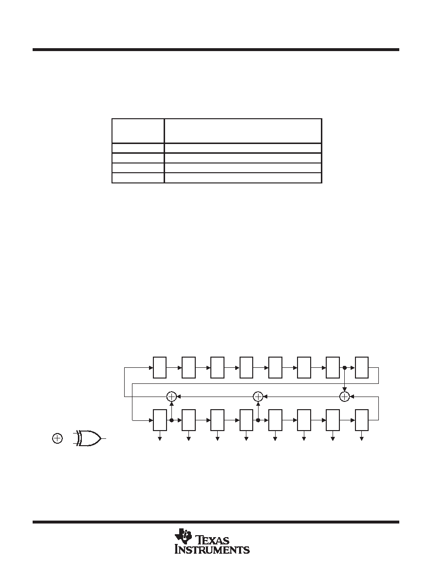
pseudo-random pattern generation (PRPG)
A pseudo-random pattern is generated in the shift-register elements of the BSCs on each rising edge of TCK
and then updated in the shadow latches and applied to the device output terminals on each falling edge of TCK.
This data is also updated in the shadow latches of the input BSCs and applied to the inputs of the normal on-chip
logic. Figure 5 illustrates the 16-bit linear-feedback shift-register algorithm through which the patterns are
generated. An initial seed value should be scanned into the BSR before performing this operation. A seed value
of all zeroes will not produce additional patterns.
=
1D
1Q
2D
3D
4D
5D
6D
7D
8D
2Q
3Q
4Q
5Q
6Q
7Q
8Q
Figure 5. 16-Bit PRPG Configuration
相關(guān)PDF資料 |
PDF描述 |
|---|---|
| SN74BCT8373ADWR | BCT/FBT SERIES, 8-BIT BOUNDARY SCAN DRIVER, TRUE OUTPUT, PDSO24 |
| SN74BCT8373NT | BCT/FBT SERIES, 8-BIT BOUNDARY SCAN DRIVER, TRUE OUTPUT, PDIP24 |
| SN74BCT8374ADWRG4 | BCT/FBT SERIES, 8-BIT BOUNDARY SCAN DRIVER, TRUE OUTPUT, PDSO24 |
| SN74BCT8374ANT | BCT/FBT SERIES, 8-BIT BOUNDARY SCAN DRIVER, TRUE OUTPUT, PDIP24 |
| SN74CB3Q16210DGVR | CB3Q/3VH/3C/2B SERIES, DUAL 10-BIT DRIVER, TRUE OUTPUT, PDSO48 |
相關(guān)代理商/技術(shù)參數(shù) |
參數(shù)描述 |
|---|---|
| SN74BCT8373ADWRG4 | 功能描述:特定功能邏輯 IEEE Std 1149.1 Bndry Scan Tst Devic RoHS:否 制造商:Texas Instruments 產(chǎn)品: 系列:SN74ABTH18502A 工作電源電壓:5 V 封裝 / 箱體:LQFP-64 封裝:Tube |
| SN74BCT8373ANT | 功能描述:特定功能邏輯 Device w/Octal D-Type Latches RoHS:否 制造商:Texas Instruments 產(chǎn)品: 系列:SN74ABTH18502A 工作電源電壓:5 V 封裝 / 箱體:LQFP-64 封裝:Tube |
| SN74BCT8373ANTE4 | 功能描述:特定功能邏輯 Device w/Octal D-Type Latches RoHS:否 制造商:Texas Instruments 產(chǎn)品: 系列:SN74ABTH18502A 工作電源電壓:5 V 封裝 / 箱體:LQFP-64 封裝:Tube |
| SN74BCT8373DW | 制造商:Rochester Electronics LLC 功能描述:- Bulk |
| SN74BCT8373DWR | 制造商:Rochester Electronics LLC 功能描述:- Bulk |
發(fā)布緊急采購,3分鐘左右您將得到回復(fù)。