- 您現(xiàn)在的位置:買賣IC網(wǎng) > PDF目錄98083 > SMJ320C40TABM40/10 (TEXAS INSTRUMENTS INC) 32-BIT, 40 MHz, OTHER DSP, UUC325 PDF資料下載
參數(shù)資料
| 型號: | SMJ320C40TABM40/10 |
| 廠商: | TEXAS INSTRUMENTS INC |
| 元件分類: | 數(shù)字信號處理 |
| 英文描述: | 32-BIT, 40 MHz, OTHER DSP, UUC325 |
| 封裝: | TAB-325 |
| 文件頁數(shù): | 48/64頁 |
| 文件大小: | 1155K |
| 代理商: | SMJ320C40TABM40/10 |
第1頁第2頁第3頁第4頁第5頁第6頁第7頁第8頁第9頁第10頁第11頁第12頁第13頁第14頁第15頁第16頁第17頁第18頁第19頁第20頁第21頁第22頁第23頁第24頁第25頁第26頁第27頁第28頁第29頁第30頁第31頁第32頁第33頁第34頁第35頁第36頁第37頁第38頁第39頁第40頁第41頁第42頁第43頁第44頁第45頁第46頁第47頁當(dāng)前第48頁第49頁第50頁第51頁第52頁第53頁第54頁第55頁第56頁第57頁第58頁第59頁第60頁第61頁第62頁第63頁第64頁
SMJ320C40, TMP320C40
DIGITAL SIGNAL PROCESSORS
SGUS017H OCTOBER 1993 REVISED OCTOBER 2001
52
POST OFFICE BOX 1443
HOUSTON, TEXAS 772511443
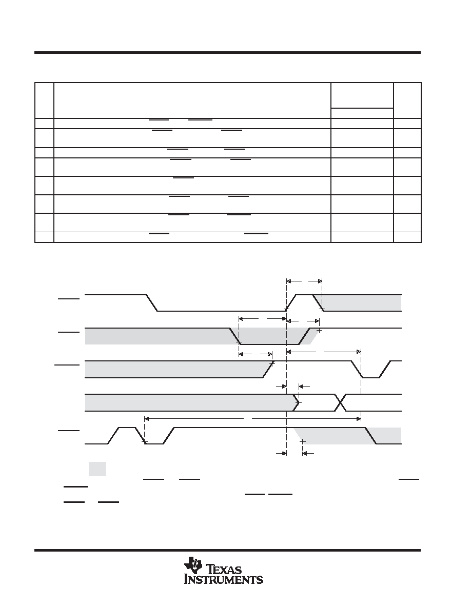
timing parameters for communication-token transfer sequence, input to an output port [P = tc(H)]
(see Figure 25)
NO.
’320C40-40*
’320C40-50*
’320C40-60*
UNIT
MIN
MAX
1
td(CAL-CS)T
Delay time, CACKx low to CSTRBx change from input to a high-level output
0.5P+ 6
1.5P+ 22
ns
2
td(CAL-CRQH)T
Delay time, CACKx low to start of CREQx going high for token-request
acknowledge
P+5
2P + 26
ns
3
td(CRQH-CRQ)T
Delay time, start of CREQx going high to CREQx change from output to an input
0.5P 5
0.5P+ 13
ns
4
td(CRQH-CA)T
Delay time, start of CREQx going high to CACKx change from an input to an
output level high
0.5P 5
0.5P+13
ns
4.1
td(CRQH-CD)T
Delay time, start of CREQx going high to CxD7 CxD0 change from inputs
driven to outputs driven
0.5P 5
0.5P+13
ns
4.2
td(CRQH-CRDY)T
Delay time, start of CREQx going high to CRDYx change from an output to an
input
0.5P 5
0.5P+13
ns
5
td(CRQH-CSL)T
Delay time, start of CREQx going high to CSTRBx low for start of word transfer
out
1.5P 8
1.5P+ 9
ns
6
td(CRDYL-CSL)T
Delay time, CRDYx low at end of word input to CSTRBx low for word output
3.5P+12
5.5P+ 48
ns
These timing parameters result from synchronizer delays and are referenced from the falling edge of H1. The inputs (that cause the output-signal
pins to change values) are sampled on H1 falling. The minimum delay occurs when the input condition occurs just before H1 falling, and the
maximum delay occurs when the input condition occurs just after H1 falling.
* On products compliant to MIL-PRF-38535, this parameter is not production tested.
CREQx
CACKx
CSTRBx
CxD7CxD0
CRDYx
= when signal is an input (clear = when signal is an output)
6
3
4
1
4.1
4.2
Valid Data Out
2
5
NOTE A: Before the token exchange, CREQx and CRDYx are output signals asserted by the SMJ320C40 that is receiving data. CACKx,
CSTRBx, and CxD7CxD0 are input signals asserted by the device sending data to the ’C40; these are asynchronous with respect to
the H1 clock of the receiving SMJ320C40. After token exchange, CACKx, CSTRBx, and CxD7CxD0 become output signals, and
CREQx and CRDYx become inputs.
Figure 25. Communication-Token Transfer Sequence, Input to an Output Port [P = tc(H)]
相關(guān)PDF資料 |
PDF描述 |
|---|---|
| SM320C40TABS60/10 | 32-BIT, 60 MHz, OTHER DSP, UUC325 |
| SMJ320C6201BGLPW20 | 32-BIT, 200 MHz, OTHER DSP, CBGA429 |
| SM320C6201BGLPW20 | 32-BIT, 200 MHz, OTHER DSP, CBGA429 |
| SMJ320C6414DGADW60 | 64-BIT, 75 MHz, OTHER DSP, CPGA570 |
| SM320C6414DGADW60 | 64-BIT, 75 MHz, OTHER DSP, CPGA570 |
相關(guān)代理商/技術(shù)參數(shù) |
參數(shù)描述 |
|---|---|
| SMJ320C40TABM50 | 制造商:未知廠家 制造商全稱:未知廠家 功能描述:32-Bit Digital Signal Processor |
| SMJ320C40TABM50/10 | 制造商:TI 制造商全稱:Texas Instruments 功能描述:DIGITAL SIGNAL PROCESSORS |
| SMJ320C40TABS60 | 制造商:未知廠家 制造商全稱:未知廠家 功能描述:32-Bit Digital Signal Processor |
| SMJ320C40TABS60/10 | 制造商:TI 制造商全稱:Texas Instruments 功能描述:DIGITAL SIGNAL PROCESSORS |
| SMJ320C40TBBM40 | 制造商:未知廠家 制造商全稱:未知廠家 功能描述:32-Bit Digital Signal Processor |
發(fā)布緊急采購,3分鐘左右您將得到回復(fù)。