- 您現(xiàn)在的位置:買賣IC網(wǎng) > PDF目錄98082 > SL28548ALC-2T PROC SPECIFIC CLOCK GENERATOR, QCC64 PDF資料下載
參數(shù)資料
| 型號(hào): | SL28548ALC-2T |
| 元件分類: | 時(shí)鐘產(chǎn)生/分配 |
| 英文描述: | PROC SPECIFIC CLOCK GENERATOR, QCC64 |
| 封裝: | 9 X 9 MM, 0.50 MM PITCH, ROHS COMPLIANT, QFN-64 |
| 文件頁(yè)數(shù): | 10/32頁(yè) |
| 文件大小: | 685K |
| 代理商: | SL28548ALC-2T |
第1頁(yè)第2頁(yè)第3頁(yè)第4頁(yè)第5頁(yè)第6頁(yè)第7頁(yè)第8頁(yè)第9頁(yè)當(dāng)前第10頁(yè)第11頁(yè)第12頁(yè)第13頁(yè)第14頁(yè)第15頁(yè)第16頁(yè)第17頁(yè)第18頁(yè)第19頁(yè)第20頁(yè)第21頁(yè)第22頁(yè)第23頁(yè)第24頁(yè)第25頁(yè)第26頁(yè)第27頁(yè)第28頁(yè)第29頁(yè)第30頁(yè)第31頁(yè)第32頁(yè)
SL28548-2
Rev 1.5 July 28, 2008
Page 18 of 32
PWRDWN# (Power down) Clarification
The CKPWRGD/PWRDWN# pin is a dual-function pin. During
initial power up, the pin functions as CKPWRGD. Once
CKPWRGD has been sampled HIGH by the clock chip, the pin
assumes PD# functionality. The PD# pin is an asynchronous
active LOW input used to shut off all clocks cleanly before
shutting off power to the device. This signal is synchronized
internally to the device before powering down the clock
synthesizer. PD# is also an asynchronous input for powering
up the system. When PD# is asserted LOW, clocks are driven
to a LOW value and held before turning off the VCOs and the
crystal oscillator.
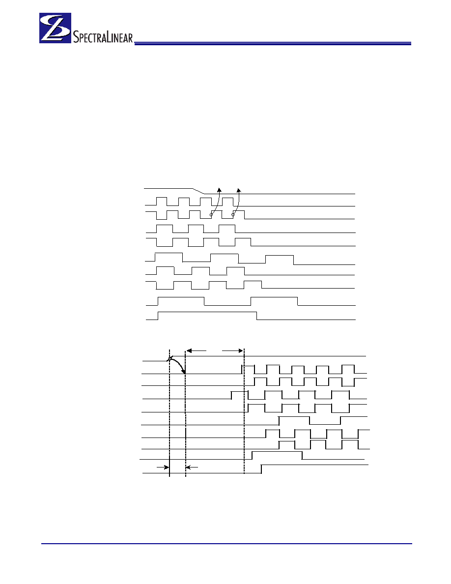
PWRDWN# (Power down) Assertion
When PD is sampled HIGH by two consecutive rising edges
of CPUC, all single-ended outputs will be held LOW on their
next HIGH-to-LOW transition and differential clocks must held
LOW. When PD mode is desired as the initial power on state,
PD must be asserted HIGH in less than 10 s after asserting
CKPWRGD.
PWRDWN# Deassertion
The power up latency is less than 1.8 ms. This is the time from
the deassertion of the PD# pin or the ramping of the power
supply until the time that stable clocks are generated from the
clock chip. All differential outputs stopped in a three-state
condition, resulting from power down are driven high in less
than 300 s of PD# deassertion to a voltage greater than
200 mV. After the clock chip’s internal PLL is powered up and
locked, all outputs are enabled within a few clock cycles of
each clock. Figure 4 is an example showing the relationship of
clocks coming up.
PD#
USB, 48MHz
DOT96T
DOT96C
SRCT 100MHz
SRCC 100MHz
CPUT, 133MHz
PCI, 33 MHz
REF
CPUC, 133MHz
Figure 3. Power down Assertion Timing Waveform
D OT 9 6 C
PD#
C P U C , 1 3 3 MH z
C P U T , 1 3 3 MH z
S R C C 1 0 0 MH z
U S B , 4 8 MH z
D OT 9 6 T
S R C T 1 0 0 MH z
Ts ta b le
< 1 .8 m s
P C I, 3 3 MH z
REF
Td r iv e _ PW R D N #
< 3 0 0 s , > 2 0 0 m V
Figure 4. Power down Deassertion Timing Waveform
相關(guān)PDF資料 |
PDF描述 |
|---|---|
| SL28610BLC | 100 MHz, PROC SPECIFIC CLOCK GENERATOR, QCC48 |
| SL28647CLCT | 400 MHz, PROC SPECIFIC CLOCK GENERATOR, QCC72 |
| SL28779CLCT | 133 MHz, PROC SPECIFIC CLOCK GENERATOR, QCC32 |
| SL28PCIE26ALIT | OTHER CLOCK GENERATOR, QCC32 |
| SL28PCIE26ALI | OTHER CLOCK GENERATOR, QCC32 |
相關(guān)代理商/技術(shù)參數(shù) |
參數(shù)描述 |
|---|---|
| SL28610BLC | 功能描述:時(shí)鐘發(fā)生器及支持產(chǎn)品 AtomPoulsbo Handheld Embed.1.5V PCIe G1 RoHS:否 制造商:Silicon Labs 類型:Clock Generators 最大輸入頻率:14.318 MHz 最大輸出頻率:166 MHz 輸出端數(shù)量:16 占空比 - 最大:55 % 工作電源電壓:3.3 V 工作電源電流:1 mA 最大工作溫度:+ 85 C 安裝風(fēng)格:SMD/SMT 封裝 / 箱體:QFN-56 |
| SL28610BLCT | 功能描述:時(shí)鐘發(fā)生器及支持產(chǎn)品 AtomPoulsbo Handheld Embed.1.5V PCIe G1 RoHS:否 制造商:Silicon Labs 類型:Clock Generators 最大輸入頻率:14.318 MHz 最大輸出頻率:166 MHz 輸出端數(shù)量:16 占空比 - 最大:55 % 工作電源電壓:3.3 V 工作電源電流:1 mA 最大工作溫度:+ 85 C 安裝風(fēng)格:SMD/SMT 封裝 / 箱體:QFN-56 |
| SL28610BLI | 功能描述:時(shí)鐘發(fā)生器及支持產(chǎn)品 AtomPoulsbo Handheld Embed.1.5V PCIe G1 RoHS:否 制造商:Silicon Labs 類型:Clock Generators 最大輸入頻率:14.318 MHz 最大輸出頻率:166 MHz 輸出端數(shù)量:16 占空比 - 最大:55 % 工作電源電壓:3.3 V 工作電源電流:1 mA 最大工作溫度:+ 85 C 安裝風(fēng)格:SMD/SMT 封裝 / 箱體:QFN-56 |
| SL28610BLIT | 功能描述:時(shí)鐘發(fā)生器及支持產(chǎn)品 AtomPoulsbo Handheld Embed.1.5V PCIe G1 RoHS:否 制造商:Silicon Labs 類型:Clock Generators 最大輸入頻率:14.318 MHz 最大輸出頻率:166 MHz 輸出端數(shù)量:16 占空比 - 最大:55 % 工作電源電壓:3.3 V 工作電源電流:1 mA 最大工作溫度:+ 85 C 安裝風(fēng)格:SMD/SMT 封裝 / 箱體:QFN-56 |
| SL28610BLITR | 制造商:Silicon Laboratories Inc 功能描述: |
發(fā)布緊急采購(gòu),3分鐘左右您將得到回復(fù)。