- 您現(xiàn)在的位置:買賣IC網(wǎng) > PDF目錄374788 > SI5364 (Electronic Theatre Controls, Inc.) SONET/SDH PRECISION PORT CARD CLOCK IC PDF資料下載
參數(shù)資料
| 型號(hào): | SI5364 |
| 廠商: | Electronic Theatre Controls, Inc. |
| 英文描述: | SONET/SDH PRECISION PORT CARD CLOCK IC |
| 中文描述: | SONET / SDH的精密端口卡時(shí)鐘IC |
| 文件頁(yè)數(shù): | 21/40頁(yè) |
| 文件大小: | 565K |
| 代理商: | SI5364 |
第1頁(yè)第2頁(yè)第3頁(yè)第4頁(yè)第5頁(yè)第6頁(yè)第7頁(yè)第8頁(yè)第9頁(yè)第10頁(yè)第11頁(yè)第12頁(yè)第13頁(yè)第14頁(yè)第15頁(yè)第16頁(yè)第17頁(yè)第18頁(yè)第19頁(yè)第20頁(yè)當(dāng)前第21頁(yè)第22頁(yè)第23頁(yè)第24頁(yè)第25頁(yè)第26頁(yè)第27頁(yè)第28頁(yè)第29頁(yè)第30頁(yè)第31頁(yè)第32頁(yè)第33頁(yè)第34頁(yè)第35頁(yè)第36頁(yè)第37頁(yè)第38頁(yè)第39頁(yè)第40頁(yè)
Si5364
Rev. 2.2
21
frequency. The FSYNC output pulse stream is time
aligned by providing a rising edge on the SYNCIN input
pin. See Figure 3 on page 6. The FSYNC output is
disabled when 255/238 FEC scaling of the clock output
frequencies is selected or when the DSBLFSYNC input
is active.
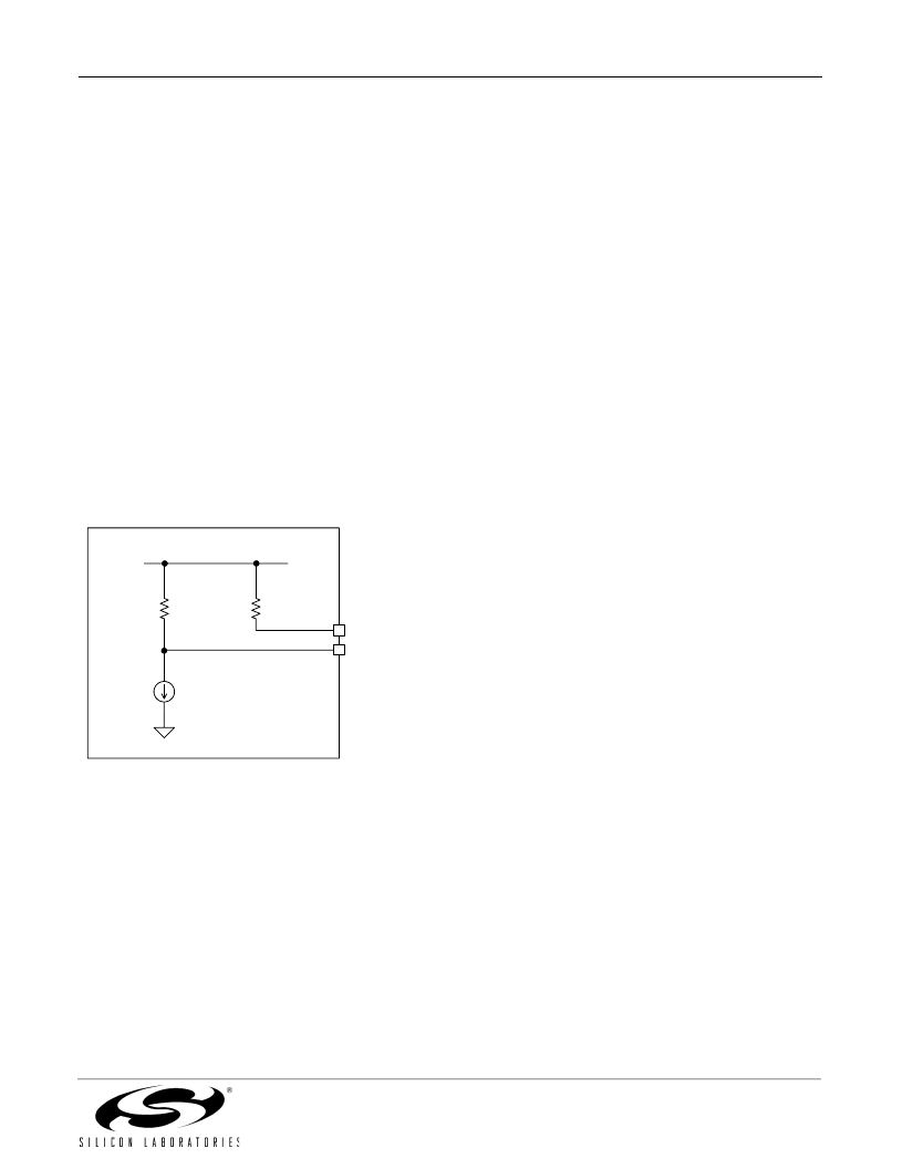
2.7. Reset
The Si5364 provides a Reset/Calibration pin, RSTN/
CAL, which resets the device and disables the outputs.
When the RSTN/CAL pin is driven low, the internal
circuitry enters into the reset mode, and all LVTTL
outputs are forced into a high impedance state. Also,
the CLKOUT_n+ and CLKOUT_n– pins are forced to a
nominal CML logic LOW and HIGH respectively (See
Figure 12). The FRQSEL_n[1:0] setting must be set to
01, 10, or 11 to enable this mode. This feature is useful
for in-circuit test applications. A low-to-high transition on
RSTN/CAL initializes all digital logic to a known
condition and initiates self-calibration of the DSPLL. At
the completion of self-calibration, the DSPLL begins to
lock to the clock input signal.
Figure 12. CLKOUT_n± Equivalent Circuit,
RSTN/CAL asserted LOW
2.8. PLL Self-Calibration
The Si5364 achieves optimal jitter performance by
using self-calibration circuitry to set the VCO center
frequency and loop gain parameters within the DSPLL.
Internal circuitry generates self calibration automatically
on powerup or after a loss-of-power condition. Self-
calibration can also be manually initiated by a low-to-
high transition on the RSTN/CAL input.
Self-calibration should be manually initiated after
changing the state of the FEC[1:0] inputs. Whether
manually initiated or automatically initiated at powerup,
the self-calibration process requires the presence of a
valid input clock.
If the self-calibration is initiated without a valid clock
present, the device waits for a valid clock before
completing the self-calibration. The Si5364 clock output
is set to the lower end of the operating frequency range
while the device waits for a valid clock. After the clock
input is validated, the calibration process runs to
completion, the device locks to the clock input, and the
clock output shifts to its target frequency. Subsequent
losses of the input clock signal do not require re-
calibration. If the clock input is lost following self-
calibration, the device enters digital hold mode. When
the input clock returns, the device re-locks to the input
clock without performing a self-calibration. During the
calibration process, the output clock frequency is
indeterminate and may jump as high as 5% above the
final locked value.
2.9. Bias Generation Circuitry
The Si5364 uses an external resistor to set internal bias
currents. The external resistor generates precise bias
currents that significantly reduce power consumption
and variation compared with traditional implementations
that use an internal resistor. The bias generation
circuitry requires a 10 k
(1%) resistor connected
between REXT and GND.
2.10. Differential Input Circuitry
The Si5364 provides differential inputs for the CLKIN_A,
CLKIN_B, and REF/CLKIN_F clock inputs. These inputs
are internally biased to a voltage of V
ICM
(see Table 2
on page 7) and are driven by differential or single-ended
driver circuits. The termination resistor is connected
externally as shown.
2.11. Differential Output Circuitry
The Si5364 uses current mode logic (CML) output
drivers to provide the clock outputs CLKOUT[3:0]. For
single-ended operation, leave one CLKOUT line
unconnected.
2.12. Power Supply Connections
The Si5364 incorporates an on-chip voltage regulator.
The
voltage
regulator
compensation circuit of one resistor and one capacitor
to ensure stability in all operating conditions.
Internally, the Si5364 V
DD33
pins are connected to the
on-chip voltage regulator input, and the V
DD33
pins also
supply power to the device’s LVTTL I/O circuitry. The
V
DD25
pins supply power to the core DSPLL circuitry
and are also used for connection of the external
compensation circuit.
The compensation circuit for the internal voltage
regulator consists of a resistor and a capacitor in series
between the V
DD25
node and ground. In practice, if a
requires
an
external
100
V
DD
2.5 V
100
CLKOUT_n–
CLKOUT_n+
15 mA
相關(guān)PDF資料 |
PDF描述 |
|---|---|
| SI5364-F-BC | SONET/SDH PRECISION PORT CARD CLOCK IC |
| SI5600 | SiPHY-TM OC-192/STM-64 SONET/SDH TRANSCEIVER |
| SI5600-BC | SiPHY-TM OC-192/STM-64 SONET/SDH TRANSCEIVER |
| SI7661 | HEATSINK TO-202 CLIP-ON .58 BK |
| SI7661DJ | HEATSINK TO-220 CLIP-ON BLK |
相關(guān)代理商/技術(shù)參數(shù) |
參數(shù)描述 |
|---|---|
| SI5364BC | 制造商:SILICON 功能描述: |
| SI5364-EVB | 功能描述:時(shí)鐘和定時(shí)器開(kāi)發(fā)工具 Multi/Jitter/Hitless 19 55 622MHz Out RoHS:否 制造商:Texas Instruments 產(chǎn)品:Evaluation Modules 類型:Clock Conditioners 工具用于評(píng)估:LMK04100B 頻率:122.8 MHz 工作電源電壓:3.3 V |
| SI5364FBC | 制造商:Vishay Siliconix 功能描述: |
| SI5364-F-BC | 功能描述:時(shí)鐘合成器/抖動(dòng)清除器 Multi/Jitter/Hitless 19 55 622MHz Outpt RoHS:否 制造商:Skyworks Solutions, Inc. 輸出端數(shù)量: 輸出電平: 最大輸出頻率: 輸入電平: 最大輸入頻率:6.1 GHz 電源電壓-最大:3.3 V 電源電壓-最小:2.7 V 封裝 / 箱體:TSSOP-28 封裝:Reel |
| SI5364-G-BC | 功能描述:時(shí)鐘發(fā)生器及支持產(chǎn)品 SONET/SDH Precision Port Card 19 155 622 RoHS:否 制造商:Silicon Labs 類型:Clock Generators 最大輸入頻率:14.318 MHz 最大輸出頻率:166 MHz 輸出端數(shù)量:16 占空比 - 最大:55 % 工作電源電壓:3.3 V 工作電源電流:1 mA 最大工作溫度:+ 85 C 安裝風(fēng)格:SMD/SMT 封裝 / 箱體:QFN-56 |
發(fā)布緊急采購(gòu),3分鐘左右您將得到回復(fù)。