- 您現(xiàn)在的位置:買賣IC網(wǎng) > PDF目錄374727 > SC416MLTRT (Semtech Corporation) Dual Synchronous Buck Controller with Tracking Start-up/Shutdown PDF資料下載
參數(shù)資料
| 型號: | SC416MLTRT |
| 廠商: | Semtech Corporation |
| 英文描述: | Dual Synchronous Buck Controller with Tracking Start-up/Shutdown |
| 中文描述: | 雙同步降壓控制器跟蹤Start-up/Shutdown |
| 文件頁數(shù): | 25/34頁 |
| 文件大?。?/td> | 1131K |
| 代理商: | SC416MLTRT |
第1頁第2頁第3頁第4頁第5頁第6頁第7頁第8頁第9頁第10頁第11頁第12頁第13頁第14頁第15頁第16頁第17頁第18頁第19頁第20頁第21頁第22頁第23頁第24頁當(dāng)前第25頁第26頁第27頁第28頁第29頁第30頁第31頁第32頁第33頁第34頁
SC416
25
The on-time pulse is programmed using the RTON resis-
tor to give a desired frequency. However, some frequen-
cy variation with line and load is expected. This variation
changes the output ripple voltage. Because constant on-
time converters regulate to the valley of the output rip-
ple, of the output ripple appears as a DC regulation er-
ror. For example, If the output ripple is 50mV with VIN = 6
volts, then the measured DC output will be 25mV above
the comparator trip point. If the ripple increases to 80mV
with VIN = 25 volts, then the measured DC output will be
40mV above the comparator trip. The best way to mini-
mize this effect is to minimize the output ripple.
To compensate for valley regulation it is often desirable
to use passive droop. Take the feedback directly from
the output side of the inductor, placing a small amount
of trace resistance between the inductor and output ca-
pacitor. This trace resistance should be optimized so that
at full load the output droops to near the lower regula-
tion limit. Passive droop minimizes the required output
capacitance because the voltage excursions due to load
steps are reduced.
The use of 1% feedback resistors contributes typically
1% error. If tighter DC accuracy is required use 0.1%
resistors. Note that for the internal preset voltages, the
FB accuracy of 1.25% for 0 to 85°C already includes the
tolerance of the internal resistors.
The output inductor value may change with current. This
will change the output ripple and thus the DC output
voltage. The output ESR also affects the ripple and thus
the DC output voltage.
Switching Frequency Variation
The switching frequency will vary somewhat due to line
and load conditions. The line variations are a result of a
fixed offset in the on-time one-shot, as well as unavoid-
able delays in the external MOSFET switching. As input
voltage increases, these factors make the actual DH on-
time slightly longer than the idealized on-time. The net
effect is that frequency tends to fall slightly with increas-
ing input voltage.
The frequency variation with load is due to losses in the
power train from IR drop and switching losses. For a con-
ventional PWM constant-frequency topology, as load
increases the duty cycle also increases slightly to com-
pensate for IR and switching losses in the MOSFETs and
inductor. A constant on-time topology must also over-
come the same losses by increasing the effective duty
cycle (more time is spent drawing energy from VIN as
losses increase). Since the on-time is constant for a given
VOUT/VIN combination, the way to increase duty cycle is
to gradually shorten the off-time. The net effect is that
switching frequency increases slightly with increasing
load.
Layout Guidelines
As with any switch-mode converter, and especially a
dual-channel converter, a good pcb layout is essential for
optimum performance. The following guidelines should
be used for PCB layout.
Placement
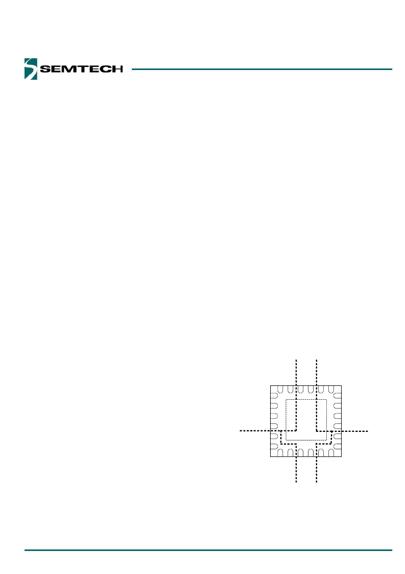
Note that the pins on the IC are arranged in four groups,
i.e. Side1 Power, Side2 Power, Side1 Analog, and Side2
Analog, as shown in Figure 21.
LX1
BST1
VDD1
DL1
EN1
SS1
LX2
BST2
VDD2
DL2
EN2
SS2
D
I
P
P
I
D
V
F
R
T
F
V
GND
(PAD)
1
7
6
12
13
18
19
24
SC416
Side 1
Power/Gate
Drive
Side 2
Power/Gate
Drive
Side 1
Analog
Side 2
Analog
Figure 21
Applications Information (continued)
相關(guān)PDF資料 |
PDF描述 |
|---|---|
| SC4201IMSTRT | Multi-Phase Link Controller |
| SC4201 | Multi-Phase Link Controller |
| SC4201EVB | Multi-Phase Link Controller |
| SC4201IMSTR | Multi-Phase Link Controller |
| SC4205IS-2.5TRT | Very Low Dropout 1 Amp Regulator With Enable |
相關(guān)代理商/技術(shù)參數(shù) |
參數(shù)描述 |
|---|---|
| SC416MLTRT/KO | 制造商:Semtech Corporation 功能描述: |
| SC416R | 功能描述:音頻指示器及警報器 CONSTANT, 4-16VDC 2900HZ, CUL APPRVD RoHS:否 制造商:PUI Audio 產(chǎn)品:Indicators 聲壓級:85 dB 音調(diào):Continuous 頻率:2300 Hz +/- 300 Hz 電壓額定值:5 VDC 電流額定值:30 mA 端接類型: 直徑:12 mm 安裝:Through Hole |
| SC417 | 制造商:SEMTECH 制造商全稱:Semtech Corporation 功能描述:10A Integrated FET Regulator with Programmable LDO |
| SC417_09 | 制造商:SEMTECH 制造商全稱:Semtech Corporation 功能描述:10A Integrated FET Regulator with Programmable LDO |
| SC417EVB | 制造商:SEMTECH 制造商全稱:Semtech Corporation 功能描述:10A Integrated FET Regulator with Programmable LDO |
發(fā)布緊急采購,3分鐘左右您將得到回復(fù)。