- 您現(xiàn)在的位置:買賣IC網(wǎng) > PDF目錄374727 > SC416MLTRT (Semtech Corporation) Dual Synchronous Buck Controller with Tracking Start-up/Shutdown PDF資料下載
參數(shù)資料
| 型號: | SC416MLTRT |
| 廠商: | Semtech Corporation |
| 英文描述: | Dual Synchronous Buck Controller with Tracking Start-up/Shutdown |
| 中文描述: | 雙同步降壓控制器跟蹤Start-up/Shutdown |
| 文件頁數(shù): | 11/34頁 |
| 文件大?。?/td> | 1131K |
| 代理商: | SC416MLTRT |
第1頁第2頁第3頁第4頁第5頁第6頁第7頁第8頁第9頁第10頁當前第11頁第12頁第13頁第14頁第15頁第16頁第17頁第18頁第19頁第20頁第21頁第22頁第23頁第24頁第25頁第26頁第27頁第28頁第29頁第30頁第31頁第32頁第33頁第34頁
SC416
11
Applications Information (continued)
Enable/Psave Inputs
Each converter has a separate Enable pin. Each EN input
operates as follows:
EN = GND. This turns the converter off.
EN = open (float). This turns the converter on with psave
mode disabled (continuous conduction mode). In this
case, the EN pin will float to approximately 2V due to
an internal 1.5Meg/1Meg resistor divider from +5V to
ground.
EN = high (3.1V min). This turns the converter on with
psave mode enabled. At light loads, the converter will
operate in psave mode.
Note that the two EN pins are separate, so each output
can be disabled or operated with or without psave inde-
pendently.
For tracking operation during startup, the two EN pins
are typically tied together; see the Voltage Tracking sec-
tion.
If both EN1 and EN2 are grounded, the device is placed
into the lowest-power state, drawing typically 7μA from
the +5V supply.
Psave Operation
Each output provides automatic psave operation at light
loads if the ENx pin is set high. The internal Zero-Cross
comparator looks for inductor current (via the voltage
across the lower MOSFET) to fall to zero on eight con-
secutive switching cycles. Once observed, the control-
ler enters psave mode and turns off the low-side MOS-
FET on each subsequent cycle when the current crosses
zero. To add hysteresis, the on-time is also increased by
25% in Psave, for that converter only; it does not affect
the other converter’s on-time. The efficiency improve-
ment at light loads more than offsets the disadvantage
of slightly higher output ripple. If the inductor current
does not cross zero on any switching cycle, the controller
immediately exits Psave. Once Psave is exited, it requires
8 switching cycles at light load to re-enter psave. Since
the controller counts zero crossings, the converter can
sink current as long as the current does not cross zero on
eight consecutive cycles. This allows the output voltage
to recover quickly in response to negative load steps.
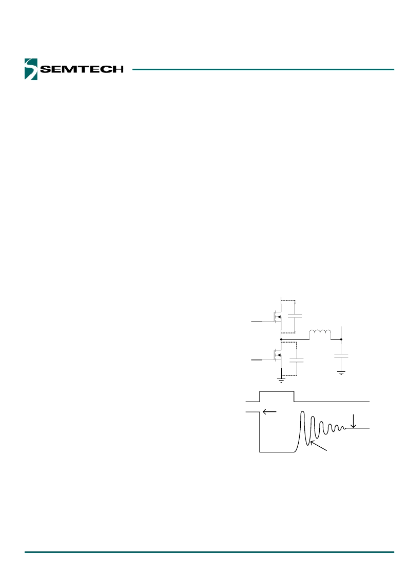
When operating in Psave mode at light loads, the LX
waveform will not have the typical square wave shape
seen when operating in continuous conduction mode.
Shortly after DL drives low, and both MOSFETs are off,
the LX voltage will show ringing. This ringing is caused
by the LC circuit formed by the inductor and device ca-
pacitance of the MOSFETs and low-side diode. When
the low-side MOSFET turns off the inductor current falls
toward zero. When it reaches zero, the inductance and
MOSFET capacitances will tend to ring freely. This is nor-
mal Psave operation as shown in Figure 3.
VOUT
VIN
COUT
L
C
Q1
C
Q2
Q1
Q2
DH
DL
DL
LX
VOUT
VIN
Typical ringing at LX
Figure 3
相關PDF資料 |
PDF描述 |
|---|---|
| SC4201IMSTRT | Multi-Phase Link Controller |
| SC4201 | Multi-Phase Link Controller |
| SC4201EVB | Multi-Phase Link Controller |
| SC4201IMSTR | Multi-Phase Link Controller |
| SC4205IS-2.5TRT | Very Low Dropout 1 Amp Regulator With Enable |
相關代理商/技術參數(shù) |
參數(shù)描述 |
|---|---|
| SC416MLTRT/KO | 制造商:Semtech Corporation 功能描述: |
| SC416R | 功能描述:音頻指示器及警報器 CONSTANT, 4-16VDC 2900HZ, CUL APPRVD RoHS:否 制造商:PUI Audio 產(chǎn)品:Indicators 聲壓級:85 dB 音調(diào):Continuous 頻率:2300 Hz +/- 300 Hz 電壓額定值:5 VDC 電流額定值:30 mA 端接類型: 直徑:12 mm 安裝:Through Hole |
| SC417 | 制造商:SEMTECH 制造商全稱:Semtech Corporation 功能描述:10A Integrated FET Regulator with Programmable LDO |
| SC417_09 | 制造商:SEMTECH 制造商全稱:Semtech Corporation 功能描述:10A Integrated FET Regulator with Programmable LDO |
| SC417EVB | 制造商:SEMTECH 制造商全稱:Semtech Corporation 功能描述:10A Integrated FET Regulator with Programmable LDO |
發(fā)布緊急采購,3分鐘左右您將得到回復。