- 您現(xiàn)在的位置:買賣IC網(wǎng) > PDF目錄385819 > SC26C92 (NXP Semiconductors N.V.) Dual universal asynchronous receiver/transmitter (DUART)(雙通用異步接收器/傳送器) PDF資料下載
參數(shù)資料
| 型號: | SC26C92 |
| 廠商: | NXP Semiconductors N.V. |
| 英文描述: | Dual universal asynchronous receiver/transmitter (DUART)(雙通用異步接收器/傳送器) |
| 中文描述: | 雙路通用異步接收器/發(fā)送器(杜阿爾特)(雙通用異步接收器/傳送器) |
| 文件頁數(shù): | 7/31頁 |
| 文件大小: | 203K |
| 代理商: | SC26C92 |
第1頁第2頁第3頁第4頁第5頁第6頁當(dāng)前第7頁第8頁第9頁第10頁第11頁第12頁第13頁第14頁第15頁第16頁第17頁第18頁第19頁第20頁第21頁第22頁第23頁第24頁第25頁第26頁第27頁第28頁第29頁第30頁第31頁
Philips Semiconductors
Product specification
SC26C92
Dual universal asynchronous receiver/transmitter (DUART)
2000 Jan 31
7
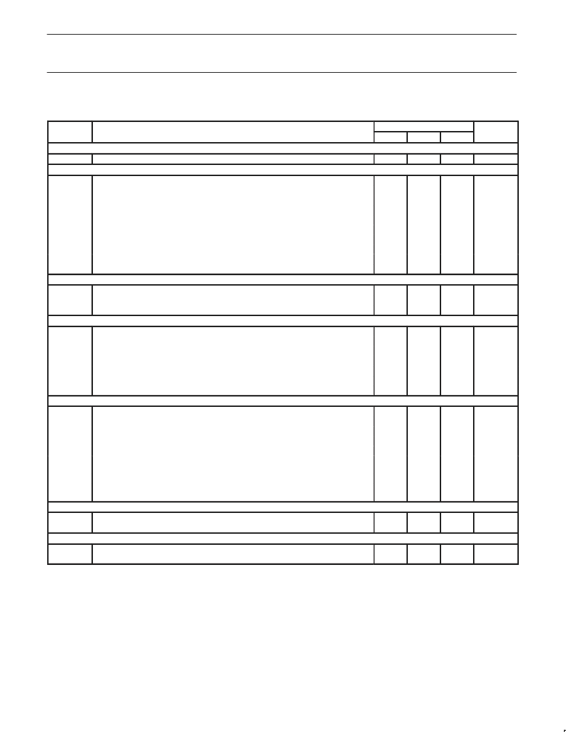
AC CHARACTERISTICS
1, 2, 4
V
CC
= 5V
±
10%, T
A
= –40 C to 85 C, unless otherwise specified.
LIMITS
Typ
3
SYMBOL
Reset Timing (See Figure 3)
t
RES
RESET pulse width
Bus Timing
5
(See Figure 4)
t
AS
A0-A3 setup time to RDN, WRN Low
t
AH
A0-A3 hold time from RDN, WRN Low
t
CS
CEN setup time to RDN, WRN Low
t
CH
CEN hold time from RDN, WRN High
t
RW
WRN, RDN pulse width
t
DD
Data valid after RDN Low
t
DF
Data bus floating after RDN High
t
DS
Data setup time before WRN or CEN High
t
DH
Data hold time after WRN or CEN High
t
RWD
High time between reads and/or writes
5, 6
Port Timing
5
(See Figure 5)
t
PS
Port input setup time before RDN Low
t
PH
Port input hold time after RDN High
t
PD
OP
n
output valid from WRN High
Interrupt Timing (See Figure 6)
INTRN (or OP3-OP7 when used as interrupts) negated from:
Read RxFIFO (RxRDY/FFULL interrupt)
Write TxFIFO (TxRDY interrupt)
t
IR
Reset command (break change interrupt)
Stop C/T command (counter interrupt)
Read IPCR (input port change interrupt)
Write IMR (clear of interrupt mask bit)
Clock Timing (See Figure 7)
t
CLK
X1/CLK High or Low time
f
CLK
X1/CLK frequency
t
CTC
CTCLK (IP2) High or Low time
f
CTC
CTCLK (IP2) frequency
t
RX
RxC High or Low time (16X)
f
RX
RxC frequency (16X)
(1X)
8
t
TX
TxC High or Low time (16X)
f
TX
TxC frequency
(16X)
(1X)
8
Transmitter Timing (See Figure 8)
t
TXD
TxD output delay from TxC external clock input on IP pin
t
TCS
Output delay from TxC low at OP pin to TxD data output
Receiver Timing (See Figure 9)
t
RXS
RxD data setup time before RxC high at external clock input on IP pin
t
RXH
RxD data hold time after RxC high at external clock input on IP pin
NOTES:
1. Parameters are valid over specified temperature range.
2. All voltage measurements are referenced to ground (GND). For testing, all inputs swing between 0.4V and 3.0V with a transition time of 5ns
maximum. For X1/CLK this swing is between 0.4V and 4.4V. All time measurements are referenced at input voltages of 0.8V and 2.0V and
output voltages of 0.8V and 2.0V, as appropriate.
3. Typical values are at +25
°
C, typical supply voltages, and typical processing parameters.
4. Test conditions for outputs: C
L
= 150pF, except interrupt outputs. Test conditions for interrupt outputs: C
L
= 50pF, R
L
= 2.7K
to V
CC
.
5. Timing is illustrated and referenced to the WRN and RDN inputs. Also, CEN may be the ‘strobing’ input. CEN and RDN (also CEN and
WRN) are ORed internally. The signal asserted last initiates the cycle and the signal negated first terminates the cycle.
6. If CEN is used as the ‘strobing’ input, the parameter defines the minimum High times between one CEN and the next. The RDN signal must
be negated for t
RWD
to guarantee that any status register changes are valid.
7. Minimum frequencies are not tested but are guaranteed by design. Crystal frequencies 2 to 4 MHz.
8. Clocks for 1X mode should be symmetrical.
PARAMETER
Min
Max
UNIT
200
ns
10
25
0
0
70
ns
ns
ns
ns
ns
ns
ns
ns
ns
ns
55
25
25
0
30
0
0
ns
ns
ns
100
100
100
100
100
100
100
ns
ns
ns
ns
ns
ns
50
0.1
55
0
30
0
0
30
0
0
ns
MHz
ns
MHz
ns
MHz
MHz
ns
MHz
MHz
3.6864
8
8
16
1
16
1
60
30
ns
ns
5
50
50
ns
ns
相關(guān)PDF資料 |
PDF描述 |
|---|---|
| SC28L92 | 3.3V- 5.0V Dual universal asynchronous receiver/transmitter (DUART)(3.3V- 5.0V雙通用異步接收器/傳送器) |
| SC3011B-1 | 600.0 MHz Differential Sine-Wave Clock |
| SC3015B | 550.0 MHz Differential Sine-Wave Clock |
| SC3017B | 400.0 MHz Differential Sine-Wave Clock |
| sc3018b | Quartz SAW Frequency Stability |
相關(guān)代理商/技術(shù)參數(shù) |
參數(shù)描述 |
|---|---|
| SC26C92A1A | 功能描述:UART 接口集成電路 UART DUAL W/FIFO RoHS:否 制造商:Texas Instruments 通道數(shù)量:2 數(shù)據(jù)速率:3 Mbps 電源電壓-最大:3.6 V 電源電壓-最小:2.7 V 電源電流:20 mA 最大工作溫度:+ 85 C 最小工作溫度:- 40 C 封裝 / 箱體:LQFP-48 封裝:Reel |
| SC26C92A1A,512 | 功能描述:UART 接口集成電路 UART DUAL W/FIFO RoHS:否 制造商:Texas Instruments 通道數(shù)量:2 數(shù)據(jù)速率:3 Mbps 電源電壓-最大:3.6 V 電源電壓-最小:2.7 V 電源電流:20 mA 最大工作溫度:+ 85 C 最小工作溫度:- 40 C 封裝 / 箱體:LQFP-48 封裝:Reel |
| SC26C92A1A,518 | 功能描述:UART 接口集成電路 5V 2 CH UART IND TEMP RoHS:否 制造商:Texas Instruments 通道數(shù)量:2 數(shù)據(jù)速率:3 Mbps 電源電壓-最大:3.6 V 電源電壓-最小:2.7 V 電源電流:20 mA 最大工作溫度:+ 85 C 最小工作溫度:- 40 C 封裝 / 箱體:LQFP-48 封裝:Reel |
| SC26C92A1A,529 | 功能描述:UART 接口集成電路 5V 2CH UART IND TEMP RoHS:否 制造商:Texas Instruments 通道數(shù)量:2 數(shù)據(jù)速率:3 Mbps 電源電壓-最大:3.6 V 電源電壓-最小:2.7 V 電源電流:20 mA 最大工作溫度:+ 85 C 最小工作溫度:- 40 C 封裝 / 箱體:LQFP-48 封裝:Reel |
| SC26C92A1A512 | 制造商:NXP Semiconductors 功能描述:IC DUAL UART FIFO 1MBPS 5.5V LCC-44 |
發(fā)布緊急采購,3分鐘左右您將得到回復(fù)。