- 您現(xiàn)在的位置:買賣IC網(wǎng) > PDF目錄374698 > SAB82532N (SIEMENS A G) ICs for Communications PDF資料下載
參數(shù)資料
| 型號: | SAB82532N |
| 廠商: | SIEMENS A G |
| 元件分類: | 微控制器/微處理器 |
| 英文描述: | ICs for Communications |
| 中文描述: | 2 CHANNEL(S), 2M bps, SERIAL COMM CONTROLLER, PQCC68 |
| 文件頁數(shù): | 13/272頁 |
| 文件大?。?/td> | 4055K |
| 代理商: | SAB82532N |
第1頁第2頁第3頁第4頁第5頁第6頁第7頁第8頁第9頁第10頁第11頁第12頁當前第13頁第14頁第15頁第16頁第17頁第18頁第19頁第20頁第21頁第22頁第23頁第24頁第25頁第26頁第27頁第28頁第29頁第30頁第31頁第32頁第33頁第34頁第35頁第36頁第37頁第38頁第39頁第40頁第41頁第42頁第43頁第44頁第45頁第46頁第47頁第48頁第49頁第50頁第51頁第52頁第53頁第54頁第55頁第56頁第57頁第58頁第59頁第60頁第61頁第62頁第63頁第64頁第65頁第66頁第67頁第68頁第69頁第70頁第71頁第72頁第73頁第74頁第75頁第76頁第77頁第78頁第79頁第80頁第81頁第82頁第83頁第84頁第85頁第86頁第87頁第88頁第89頁第90頁第91頁第92頁第93頁第94頁第95頁第96頁第97頁第98頁第99頁第100頁第101頁第102頁第103頁第104頁第105頁第106頁第107頁第108頁第109頁第110頁第111頁第112頁第113頁第114頁第115頁第116頁第117頁第118頁第119頁第120頁第121頁第122頁第123頁第124頁第125頁第126頁第127頁第128頁第129頁第130頁第131頁第132頁第133頁第134頁第135頁第136頁第137頁第138頁第139頁第140頁第141頁第142頁第143頁第144頁第145頁第146頁第147頁第148頁第149頁第150頁第151頁第152頁第153頁第154頁第155頁第156頁第157頁第158頁第159頁第160頁第161頁第162頁第163頁第164頁第165頁第166頁第167頁第168頁第169頁第170頁第171頁第172頁第173頁第174頁第175頁第176頁第177頁第178頁第179頁第180頁第181頁第182頁第183頁第184頁第185頁第186頁第187頁第188頁第189頁第190頁第191頁第192頁第193頁第194頁第195頁第196頁第197頁第198頁第199頁第200頁第201頁第202頁第203頁第204頁第205頁第206頁第207頁第208頁第209頁第210頁第211頁第212頁第213頁第214頁第215頁第216頁第217頁第218頁第219頁第220頁第221頁第222頁第223頁第224頁第225頁第226頁第227頁第228頁第229頁第230頁第231頁第232頁第233頁第234頁第235頁第236頁第237頁第238頁第239頁第240頁第241頁第242頁第243頁第244頁第245頁第246頁第247頁第248頁第249頁第250頁第251頁第252頁第253頁第254頁第255頁第256頁第257頁第258頁第259頁第260頁第261頁第262頁第263頁第264頁第265頁第266頁第267頁第268頁第269頁第270頁第271頁第272頁
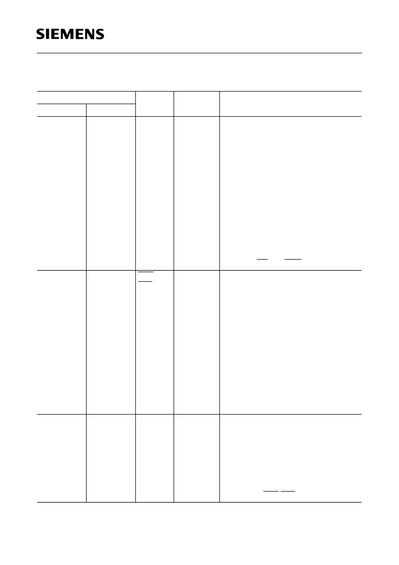
SAB 82532/SAF 82532
Introduction
Semiconductor Group
13
07.96
28
63
RES
I
Reset
A high signal on this pin forces the ESCC2
into reset state. During Reset the ESCC2
is in power up mode, after Reset in
power-down mode. Re-activation of each
channel is done via bit CCR0:PU (refer to
chapter 9.2
).
During Reset
– all uni-directional output stages are in
high-impedance state,
– all bi-directional output stages (data
bus) are in high-impedance state,
– output XTAL2 is in high-impedance if
input XTAL1 is ‘high’ (the internal
oscillator is disabled during reset),
– signals RD and INTA have to be ‘high’
10
42
BHE/
BLE
I
Bus High Enable
(Siemens/Intel bus mode)
If 16-bit bus interface mode is enabled,
this signal indicates a data transfer on the
upper byte of the data bus (D8…D15). In
8-bit bus interface mode this signal has no
function and should be tied to
V
DD
. Refer
to
chapter 3.1
for detailed information.
Bus Low Enable
(Motorola bus mode)
If 16-bit bus interface mode is enabled,
this signal indicates a data transfer on the
lower byte of the data bus (D0 … D7). In
8-bit bus interface mode this signal has no
function and should be tied to
V
DD
. Refer
to
chapter 3.1
for detailed information.
29
64
WIDTH
I
Width Of Bus Interface
(Bus Interface Mode)
A low signal on this input selects the 8-bit
bus interface mode. A high signal on this
input selects the 16-bit bus interface
mode. In this case word transfer to/from
the internal registers is enabled.
Moreover, byte transfers (in conjunction
with A0 and BHE/BLE) are allowed, too.
1.3
Pin Definitions and Functions
(cont’d)
Pin No.
Symbol
Input (I)
Output (O)
Function
P-LCC-68
P-MQFP-80
相關PDF資料 |
PDF描述 |
|---|---|
| SAB82532N-10 | ICs for Communications |
| SAF82532 | ICs for Communications |
| SAF82532N-10 | ICs for Communications |
| SAB82532H-10 | ICs for Communications |
| SAFC161U | Embedded C166 with USB, USART and SSC |
相關代理商/技術參數(shù) |
參數(shù)描述 |
|---|---|
| SAB82532N V2.2 | 制造商:Siemens 功能描述: |
| SAB82532N-10 | 制造商:Siemens 功能描述:2 CHANNEL(S), 10M BPS, MULTI PROTOCOL CONTROLLER, PQCC68 |
| SAB82532N10V2.2 | 制造商:Infineon Technologies AG 功能描述: |
| SAB82532N-10V2.2 | 制造商:Siemens 功能描述:2 CHANNEL(S), 10M BPS, MULTI PROTOCOL CONTROLLER, PQCC68 |
| SAB82532N-10V3.2A | 制造商:Siemens 功能描述:Part Number Only |
發(fā)布緊急采購,3分鐘左右您將得到回復。