- 您現(xiàn)在的位置:買賣IC網(wǎng) > PDF目錄382382 > PCF8576CH (NXP SEMICONDUCTORS) Universal LCD driver for low multiplex rates PDF資料下載
參數(shù)資料
| 型號(hào): | PCF8576CH |
| 廠商: | NXP SEMICONDUCTORS |
| 元件分類: | 顯示驅(qū)動(dòng)器 |
| 英文描述: | Universal LCD driver for low multiplex rates |
| 中文描述: | LIQUID CRYSTAL DISPLAY DRIVER, PQFP64 |
| 封裝: | 10 X 10 MM, 1.40 MM HEIGHT, PLASTIC, MS-026, SOT314-2, LQFP-64 |
| 文件頁數(shù): | 15/40頁 |
| 文件大小: | 243K |
| 代理商: | PCF8576CH |
第1頁第2頁第3頁第4頁第5頁第6頁第7頁第8頁第9頁第10頁第11頁第12頁第13頁第14頁當(dāng)前第15頁第16頁第17頁第18頁第19頁第20頁第21頁第22頁第23頁第24頁第25頁第26頁第27頁第28頁第29頁第30頁第31頁第32頁第33頁第34頁第35頁第36頁第37頁第38頁第39頁第40頁

1998 Feb 06
15
Philips Semiconductors
Product specification
Universal LCD driver for low multiplex
rates
PCF8576
6.9
Segment outputs
The LCD drive section includes 40 segment outputs
pins S0 to S39 which should be connected directly to the
LCD. The segment output signals are generated in
accordance with the multiplexed backplane signals and
with data resident in the display latch. When less than
40 segment outputs are required the unused segment
outputs should be left open-circuit.
6.10
Backplane outputs
The LCD drive section includes four backplane outputs
BP0 to BP3 which should be connected directly to the
LCD. The backplane output signals are generated in
accordance with the selected LCD drive mode. If less than
four backplane outputs are required the unused outputs
can be left open-circuit. In the 1 : 3 multiplex drive mode
BP3 carries the same signal as BP1, therefore these two
adjacent outputs can be connected together to give
enhanced drive capabilities. In the 1 : 2 multiplex drive
mode BP0 and BP2, BP1 and BP3 respectively carry the
same signals and may also be paired to increase the drive
capabilities. In the static drive mode the same signal is
carried by all four backplane outputs and they can be
connected in parallel for very high drive requirements.
6.11
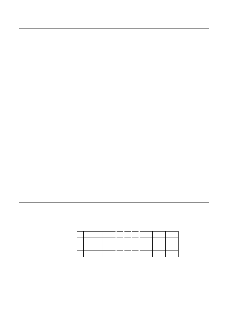
Display RAM
The display RAM is a static 40
×
4-bit RAM which stores
LCD data. A logic 1 in the RAM bit-map indicates the on
state of the corresponding LCD segment; similarly, a
logic 0 indicates the off state. There is a one-to-one
correspondence between the RAM addresses and the
segment outputs, and between the individual bits of a RAM
word and the backplane outputs. The first RAM column
corresponds to the 40 segments operated with respect to
backplane BP0 (see Fig.10). In multiplexed LCD
applications the segment data of the second, third and
fourth column of the display RAM are time-multiplexed
with BP1, BP2 and BP3 respectively.
When display data is transmitted to the PCF8576 the
display bytes received are stored in the display RAM in
accordance with the selected LCD drive mode.
To illustrate the filling order, an example of a 7-segment
numeric display showing all drive modes is given in Fig.11;
the RAM filling organization depicted applies equally to
other LCD types.
With reference to Fig.11, in the static drive mode the eight
transmitted data bits are placed in bit 0 of eight successive
display RAM addresses. In the 1 : 2 multiplex drive mode
the eight transmitted data bits are placed in bits 0 and 1 of
four successive display RAM addresses. In the 1 : 3
multiplex drive mode these bits are placed in
bits 0, 1 and 2 of three successive addresses, with bit 2 of
the third address left unchanged. This last bit may, if
necessary, be controlled by an additional transfer to this
address but care should be taken to avoid overriding
adjacent data because full bytes are always transmitted.
In the 1 : 4 multiplex drive mode the eight transmitted data
bits are placed in bits 0, 1, 2 and 3 of two successive
display RAM addresses.
Fig.10 Display RAM bit-map showing direct relationship between display RAM addresses and segment outputs,
and between bits in a RAM word and backplane outputs.
0
0
1
2
3
1
2
3
4
35
36
37
38
39
display RAM addresses (rows) / segment outputs (S)
display RAM bits
(columns) /
backplane outputs
(BP)
MBE525
相關(guān)PDF資料 |
PDF描述 |
|---|---|
| PCF8576U | Universal LCD driver for low multiplex rates |
| PCF8577C | LCD direct/duplex driver with I2C-bus interface |
| PCF8577CP | LCD direct/duplex driver with I2C-bus interface |
| PCF8591 | 8-bit A/D and D/A converter |
| PCA8591 | 8-bit A/D and D/A converter |
相關(guān)代理商/技術(shù)參數(shù) |
參數(shù)描述 |
|---|---|
| PCF8576CH/1 | 功能描述:LCD 驅(qū)動(dòng)器 160 SEGMENT LCD SEGMENT DRIVER RoHS:否 制造商:Maxim Integrated 數(shù)位數(shù)量:4.5 片段數(shù)量:30 最大時(shí)鐘頻率:19 KHz 工作電源電壓:3 V to 3.6 V 最大工作溫度:+ 85 C 最小工作溫度:- 20 C 封裝 / 箱體:PDIP-40 封裝:Tube |
| PCF8576CH/1,118 | 功能描述:LCD 驅(qū)動(dòng)器 160 SEGMENT LCD SEGMENT DRIVER RoHS:否 制造商:Maxim Integrated 數(shù)位數(shù)量:4.5 片段數(shù)量:30 最大時(shí)鐘頻率:19 KHz 工作電源電壓:3 V to 3.6 V 最大工作溫度:+ 85 C 最小工作溫度:- 20 C 封裝 / 箱體:PDIP-40 封裝:Tube |
| PCF8576CH/1,157 | 功能描述:LCD 驅(qū)動(dòng)器 160 SEGMENT LCD RoHS:否 制造商:Maxim Integrated 數(shù)位數(shù)量:4.5 片段數(shù)量:30 最大時(shí)鐘頻率:19 KHz 工作電源電壓:3 V to 3.6 V 最大工作溫度:+ 85 C 最小工作溫度:- 20 C 封裝 / 箱體:PDIP-40 封裝:Tube |
| PCF8576CHBD-S | 制造商:未知廠家 制造商全稱:未知廠家 功能描述:LCD Display Driver |
| PCF8576CHL/1 | 制造商:NXP Semiconductors 功能描述:LCD DRIVER 64LQFP 制造商:NXP Semiconductors 功能描述:LCD DRIVER, 64LQFP 制造商:NXP Semiconductors 功能描述:LCD DRIVER, 64LQFP; No. of Digits / Alpha:10; No. of Segments:40; Driver Case Style:LQFP; No. of Pins:64; Supply Voltage Min:2V; Supply Voltage Max:6V; Interface Type:I2C; Operating Temperature Min:-40C; Operating Temperature ;RoHS Compliant: Yes |
發(fā)布緊急采購,3分鐘左右您將得到回復(fù)。