- 您現(xiàn)在的位置:買賣IC網(wǎng) > PDF目錄382381 > PCF2105 (NXP Semiconductors N.V.) LCD controller/driver PDF資料下載
參數(shù)資料
| 型號: | PCF2105 |
| 廠商: | NXP Semiconductors N.V. |
| 英文描述: | LCD controller/driver |
| 中文描述: | LCD控制器/驅(qū)動器 |
| 文件頁數(shù): | 11/48頁 |
| 文件大小: | 289K |
| 代理商: | PCF2105 |
第1頁第2頁第3頁第4頁第5頁第6頁第7頁第8頁第9頁第10頁當(dāng)前第11頁第12頁第13頁第14頁第15頁第16頁第17頁第18頁第19頁第20頁第21頁第22頁第23頁第24頁第25頁第26頁第27頁第28頁第29頁第30頁第31頁第32頁第33頁第34頁第35頁第36頁第37頁第38頁第39頁第40頁第41頁第42頁第43頁第44頁第45頁第46頁第47頁第48頁
1998 Jul 30
11
Philips Semiconductors
Product specification
LCD controller/driver
PCF2105
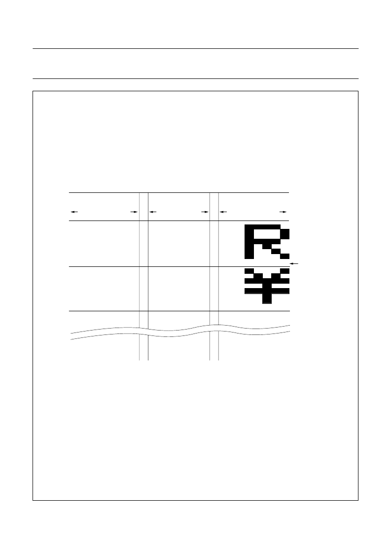
Fig.6 Relationship between CGRAM addresses, data and display patterns.
Character code bits 0 to 3 correspond to CGRAM address bits 3 to 6.
CGRAM address bits 0 to 2 designate character pattern line position. The 8th line is the cursor position and display is performed by logical OR with the
cursor. Data in the 8th line will appear in the cursor position.
Character pattern column positions correspond to CGRAM data bits 0 to 4; bit 4 being at the left end, as shown in this figure.
CGRAM character patterns are selected when character code bits 4 to 7 are all logic 0. CGRAM data is logic 1 corresponds to selection for display.
Only bits 0 to 5 of the CGRAM address are set by the ‘set CGRAM address’ instruction. Bit 6 can be set using the ‘set DDRAM address’ instruction or
by using the auto-increment feature during CGRAM write. All bits 0 to 6 can be read using the ‘read busy flag and address’ instruction.
handbook, full pagewidth
MGA800 - 1
7
6
5
4
3
2
1
0
6
5
4
3
2
1
0
4
3
2
1
0
higher
order
bits
lower
order
bits
lower
order
bits
higher
order
bits
lower
order
bits
higher
order
bits
0
0
0
0
0
0
0
0
0
0
0
0
0
0
0
0
1
1
1
1
0
0
1
1
0
0
1
1
0
1
0
1
0
1
0
1
0
0
0
0
0
0
0
0
0
0
0
0
0
0
0
0
0
0
0
0
0
0
0
0
0
0
1
1
1
1
0
0
1
1
0
0
1
1
0
1
0
1
0
1
0
1
0
0
0
0
0
0
0
0
0
0
0
0
0
0
0
0
0
0
0
0
0
0
0
0
0
1
0
0
0
0
0
0
0
1
0
0
0
1
0
0
0
0
0
0
1
0
0
0
0
0
0
0
0
0
0
0
0
0
0
0
0
0
1
1
1
1
1
1
1
1
1
1
1
1
1
1
1
1
0
1
0
0
0
0
0
1
1
1
1
0
0
1
1
0
1
0
1
1
1
1
1
1
1
1
1
1
1
1
1
1
1
1
1
character codes
(DDRAM data)
CGRAM
address
character patterns
(CGRAM data)
character
pattern
example 1
cursor
position
character
pattern
example 2
相關(guān)PDF資料 |
PDF描述 |
|---|---|
| PCF2105MU | LCD controller/driver |
| PCF26100 | Bluetooth Adapter IC |
| PCF26100ET | DVI_D - DVI_D SINGLE LINK CABLE 5M BLK RoHS Compliant: Yes |
| PCF3F10B | Analog IC |
| PCF3F160 | Analog IC |
相關(guān)代理商/技術(shù)參數(shù) |
參數(shù)描述 |
|---|---|
| PCF2105MU | 制造商:PHILIPS 制造商全稱:NXP Semiconductors 功能描述:LCD controller/driver |
| PCF2105MU/2 | 制造商:PHILIPS 制造商全稱:NXP Semiconductors 功能描述:LCD controller/driver |
| PCF2105MU/7 | 制造商:未知廠家 制造商全稱:未知廠家 功能描述:LCD Display Driver |
| PCF210AA | 制造商:PHILIPS 制造商全稱:NXP Semiconductors 功能描述:SPI Real time clock/calendar Time keeping application |
| PCF2110 | 制造商:未知廠家 制造商全稱:未知廠家 功能描述:LCD Display Driver |
發(fā)布緊急采購,3分鐘左右您將得到回復(fù)。