- 您現在的位置:買賣IC網 > PDF目錄382381 > PCD8544U (NXP SEMICONDUCTORS) 48 x 84 pixels matrix LCD controller/driver PDF資料下載
參數資料
| 型號: | PCD8544U |
| 廠商: | NXP SEMICONDUCTORS |
| 元件分類: | 顯示驅動器 |
| 英文描述: | 48 x 84 pixels matrix LCD controller/driver |
| 中文描述: | LIQUID CRYSTAL DISPLAY DRIVER, UUC168 |
| 封裝: | BUMP, DIE-168 |
| 文件頁數: | 11/32頁 |
| 文件大?。?/td> | 154K |
| 代理商: | PCD8544U |
第1頁第2頁第3頁第4頁第5頁第6頁第7頁第8頁第9頁第10頁當前第11頁第12頁第13頁第14頁第15頁第16頁第17頁第18頁第19頁第20頁第21頁第22頁第23頁第24頁第25頁第26頁第27頁第28頁第29頁第30頁第31頁第32頁

1999 Apr 12
11
Philips Semiconductors
Product specification
48
×
84 pixels matrix LCD controller/driver
PCD8544
8
INSTRUCTIONS
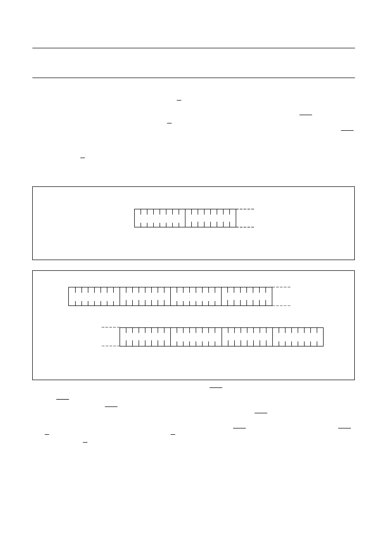
The instruction format is divided into two modes: If D/C
(mode select) is set LOW, the current byte is interpreted as
command byte (see Table 1). Figure 8 shows an example
of a serial data stream for initializing the chip. If D/C is set
HIGH, the following bytes are stored in the display data
RAM. After every data byte, the address counter is
incremented automatically.
The level of the D/C signal is read during the last bit of data
byte.
Each instruction can be sent in any order to the PCD8544.
The MSB of a byte is transmitted first. Figure 9 shows one
possible command stream, used to set up the LCD driver.
The serial interface is initialized when SCE is HIGH. In this
state, SCLK clock pulses have no effect and no power is
consumed by the serial interface. A negative edge on SCE
enables the serial interface and indicates the start of a data
transmission.
Fig.8 General format of data stream.
handbook, halfpage
MGL666
data
data
LSB (DB0)
Fig.9 Serial data stream, example.
handbook, full pagewidth
MGL642
function set (H = 1)
bias system
set VOP
temperature control
function set (H = 0)
display control
X address
Y address
Figures 10 and 11 show the serial bus protocol.
When SCE is HIGH, SCLK clock signals are ignored;
during the HIGH time of SCE, the serial interface is
initialized (see Fig.12)
SDIN is sampled at the positive edge of SCLK
D/C indicates whether the byte is a command (D/C = 0)
or RAM data (D/C = 1); it is read with the eighth SCLK
pulse
If SCE stays LOW after the last bit of a command/data
byte, the serial interface expects bit 7 of the next byte at
the next positive edge of SCLK (see Fig.12)
A reset pulse with RES interrupts the transmission.
No data is written into the RAM. The registers are
cleared. If SCE is LOW after the positive edge of RES,
the serial interface is ready to receive bit 7 of a
command/data byte (see Fig.13).
相關PDF資料 |
PDF描述 |
|---|---|
| PCDAC12-4 | PC(ISA)BUS I/O CARD |
| PCDBM | Power Conversion dBm to Watts |
| PCE84C486 | Microcontrollers for digital auto-sync and VST TV controller applications |
| PCE84C487 | Microcontrollers for digital auto-sync and VST TV controller applications |
| PCE84C886 | Microcontroller for monitor OSD and auto-sync applications |
相關代理商/技術參數 |
參數描述 |
|---|---|
| PCD8572 | 制造商:Rochester Electronics LLC 功能描述:- Bulk 制造商:Microchip Technology Inc 功能描述: |
| PCD8572/J | 制造商:未知廠家 制造商全稱:未知廠家 功能描述:I2C Serial EEPROM |
| PCD8572/P | 制造商:Rochester Electronics LLC 功能描述:- Bulk 制造商:Microchip Technology Inc 功能描述: |
| PCD8572/P010 | 制造商:Rochester Electronics LLC 功能描述:- Bulk 制造商:Microchip Technology Inc 功能描述: |
| PCD8572I | 制造商:Rochester Electronics LLC 功能描述:- Bulk |
發(fā)布緊急采購,3分鐘左右您將得到回復。