- 您現(xiàn)在的位置:買賣IC網(wǎng) > PDF目錄299581 > ORLI10G2BM680-DB (LATTICE SEMICONDUCTOR CORP) FPGA, 1296 CLBS, 333000 GATES, PBGA680 PDF資料下載
參數(shù)資料
| 型號: | ORLI10G2BM680-DB |
| 廠商: | LATTICE SEMICONDUCTOR CORP |
| 元件分類: | FPGA |
| 英文描述: | FPGA, 1296 CLBS, 333000 GATES, PBGA680 |
| 封裝: | PLASTIC, FBGA-680 |
| 文件頁數(shù): | 26/78頁 |
| 文件大小: | 1689K |
| 代理商: | ORLI10G2BM680-DB |
第1頁第2頁第3頁第4頁第5頁第6頁第7頁第8頁第9頁第10頁第11頁第12頁第13頁第14頁第15頁第16頁第17頁第18頁第19頁第20頁第21頁第22頁第23頁第24頁第25頁當(dāng)前第26頁第27頁第28頁第29頁第30頁第31頁第32頁第33頁第34頁第35頁第36頁第37頁第38頁第39頁第40頁第41頁第42頁第43頁第44頁第45頁第46頁第47頁第48頁第49頁第50頁第51頁第52頁第53頁第54頁第55頁第56頁第57頁第58頁第59頁第60頁第61頁第62頁第63頁第64頁第65頁第66頁第67頁第68頁第69頁第70頁第71頁第72頁第73頁第74頁第75頁第76頁第77頁第78頁
Lattice Semiconductor
ORCA ORLI10G Data Sheet
32
XGMII ORCA 4E Receive Analysis
XGMII Considerations
The stringent 10 Gbit Media Independent Interface (XGMII) specications from the IEEE 802.3ae standards are
met in the FPGA side of the ORLI10G device. This interface is implemented in the PCS IP core and targeted to the
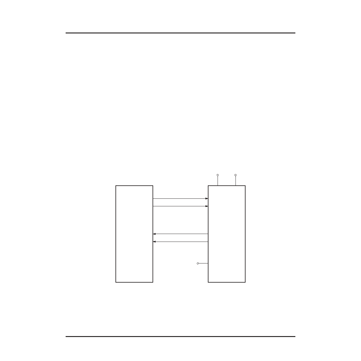
ORLI10G FPSC. Figure 18 shows a simplied block diagram for the XGMII interface. Other I/O standards are also
possible, such as SSTL or HSTL, with a reference voltage of 1.8 V. Further details are available in the Series 4 I/O
application note and the Series 4 Fast Input DDR and Output DDR with Clock Forwarding Application Note.
The ORLI10G device meets the 480 ps input setup time and 480 ps input hold time requirements for the XGMII
receiver inputs into the FPGA side of the FPSC with the embedded I/O DDR cells on the FPGA side of the FPSC.
The PLLs are not used on input because this is a forward clocked interface. The ORLI10G meets the clock-to-out
specication on the XGMII DDR outputs by using the output shift register to produce a non-duty-cycle-dependent
output. An embedded output DDR capability is also available. The output clock is then centered around this data
eye using internal PLLs.
There are two considerations to note about the pinout location of the XGMII input clocks:
1.
The XGMII input clocks must be located at the C pad of the programmable I/O cells (PICs). In the pinout tables,
the pads are labeled on a pin-by-pin basis. For example, a pin whose pad is referenced as PL1C can be used
as an XGMII input clock, but pins referenced as PL1A, PL1B, or PL1D cannot be used as an XGMII input clock.
2.
The XGMII input data pins can be no further then six PICs away from the XGMII input clock pin.
Figure 18. Simplied XGMII Block Diagram
HSTL
CLOCK
VDDIO
VDD15
VDDIO = 1.5 V NOM
HSTL
VDDIO = 1.5 V NOM
VREF
VDDIO ÷ 2
DDR DATA
CUSTOMER DEVICE
ORLI10G
SYSTEM
INTERFACE
LINE
INTERFACE
相關(guān)PDF資料 |
PDF描述 |
|---|---|
| ORLI10G3BM680-DB | FPGA, 1296 CLBS, 333000 GATES, PBGA680 |
| ORT82G5-1BM680 | FPGA, 1296 CLBS, 380000 GATES, PBGA680 |
| ORT82G5-2BM680 | FPGA, 1296 CLBS, 380000 GATES, PBGA680 |
| ORT82G5-3BM680 | FPGA, 1296 CLBS, 380000 GATES, PBGA680 |
| OS10040280G-012 | FIBER OPTIC RECEIVER, 1290-1600nm, PANEL MOUNT, FC/APC CONNECTOR |
相關(guān)代理商/技術(shù)參數(shù) |
參數(shù)描述 |
|---|---|
| ORLI10G-2BM680I | 功能描述:FPGA - 現(xiàn)場可編程門陣列 10368 LUT 316 I/O RoHS:否 制造商:Altera Corporation 系列:Cyclone V E 柵極數(shù)量: 邏輯塊數(shù)量:943 內(nèi)嵌式塊RAM - EBR:1956 kbit 輸入/輸出端數(shù)量:128 最大工作頻率:800 MHz 工作電源電壓:1.1 V 最大工作溫度:+ 70 C 安裝風(fēng)格:SMD/SMT 封裝 / 箱體:FBGA-256 |
| ORLI10G-2BMN680C | 功能描述:FPGA - 現(xiàn)場可編程門陣列 10368 LUT 316 I/O RoHS:否 制造商:Altera Corporation 系列:Cyclone V E 柵極數(shù)量: 邏輯塊數(shù)量:943 內(nèi)嵌式塊RAM - EBR:1956 kbit 輸入/輸出端數(shù)量:128 最大工作頻率:800 MHz 工作電源電壓:1.1 V 最大工作溫度:+ 70 C 安裝風(fēng)格:SMD/SMT 封裝 / 箱體:FBGA-256 |
| ORLI10G-2BMN680I | 功能描述:FPGA - 現(xiàn)場可編程門陣列 10368 LUT 316 I/O RoHS:否 制造商:Altera Corporation 系列:Cyclone V E 柵極數(shù)量: 邏輯塊數(shù)量:943 內(nèi)嵌式塊RAM - EBR:1956 kbit 輸入/輸出端數(shù)量:128 最大工作頻率:800 MHz 工作電源電壓:1.1 V 最大工作溫度:+ 70 C 安裝風(fēng)格:SMD/SMT 封裝 / 箱體:FBGA-256 |
| ORLI10G-3BM680C | 功能描述:FPGA - 現(xiàn)場可編程門陣列 10368 LUT 316 I/O RoHS:否 制造商:Altera Corporation 系列:Cyclone V E 柵極數(shù)量: 邏輯塊數(shù)量:943 內(nèi)嵌式塊RAM - EBR:1956 kbit 輸入/輸出端數(shù)量:128 最大工作頻率:800 MHz 工作電源電壓:1.1 V 最大工作溫度:+ 70 C 安裝風(fēng)格:SMD/SMT 封裝 / 箱體:FBGA-256 |
| ORLI10G-3BMN680C | 功能描述:FPGA - 現(xiàn)場可編程門陣列 10368 LUT 316 I/O RoHS:否 制造商:Altera Corporation 系列:Cyclone V E 柵極數(shù)量: 邏輯塊數(shù)量:943 內(nèi)嵌式塊RAM - EBR:1956 kbit 輸入/輸出端數(shù)量:128 最大工作頻率:800 MHz 工作電源電壓:1.1 V 最大工作溫度:+ 70 C 安裝風(fēng)格:SMD/SMT 封裝 / 箱體:FBGA-256 |
發(fā)布緊急采購,3分鐘左右您將得到回復(fù)。
