- 您現(xiàn)在的位置:買賣IC網(wǎng) > PDF目錄299581 > ORLI10G-3BM680 (LATTICE SEMICONDUCTOR CORP) FPGA, 1296 CLBS, 380000 GATES, PBGA680 PDF資料下載
參數(shù)資料
| 型號: | ORLI10G-3BM680 |
| 廠商: | LATTICE SEMICONDUCTOR CORP |
| 元件分類: | FPGA |
| 英文描述: | FPGA, 1296 CLBS, 380000 GATES, PBGA680 |
| 封裝: | PLASTIC, BGA-680 |
| 文件頁數(shù): | 43/76頁 |
| 文件大?。?/td> | 1222K |
| 代理商: | ORLI10G-3BM680 |
第1頁第2頁第3頁第4頁第5頁第6頁第7頁第8頁第9頁第10頁第11頁第12頁第13頁第14頁第15頁第16頁第17頁第18頁第19頁第20頁第21頁第22頁第23頁第24頁第25頁第26頁第27頁第28頁第29頁第30頁第31頁第32頁第33頁第34頁第35頁第36頁第37頁第38頁第39頁第40頁第41頁第42頁當前第43頁第44頁第45頁第46頁第47頁第48頁第49頁第50頁第51頁第52頁第53頁第54頁第55頁第56頁第57頁第58頁第59頁第60頁第61頁第62頁第63頁第64頁第65頁第66頁第67頁第68頁第69頁第70頁第71頁第72頁第73頁第74頁第75頁第76頁
48
Lattice Semiconductor
Data Sheet
January 15, 2002
and ORLI12G Gbits/s Line Interface FPSC
ORCA ORLI10G Quad 2.5 Gbits/s, 10 Gbits/s
Pin Information (continued)
Package Pinouts
Table 14 provides the number of user-programmable I/
Os available for each available package. Table 20 pro-
vides the package pin and pin function for the
ORLI10G FPSC and packages. The bond pad name is
identied in the PIO nomenclature used in the ORCA
Foundry design editor. The bank column provides infor-
mation as to which output voltage level bank the given
pin is in. The group column provides information as to
the group of pins the given pin is in. This is used to
show which VREF pin is used to provide the reference
voltage for single-ended limited-swing I/Os. If none of
these buffer types (such as SSTL, GTL, HSTL) are
used in a given group, then the VREF pin is available
as an I/O pin.
When the number of FPGA bond pads exceeds the
number of package pins, bond pads are unused. When
the number of package pins exceeds the number of
bond pads, package pins are left unconnected (no con-
nects). When a package pin is to be left as a no con-
nect for a specic die, it is indicated as a note in the
device column for the FPGA. The tables provide no
information on unused pads.
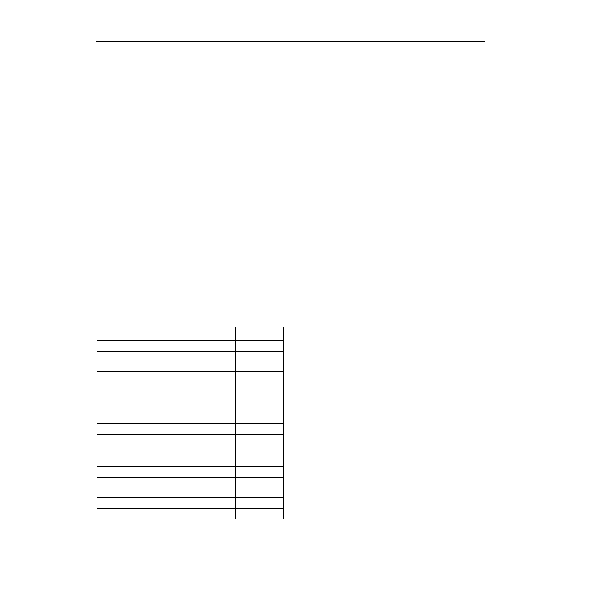
Table 18. ORCA Programmable I/Os Summary
It is very important to note the pinout limitations for 10
Gbits/s Ethernet applications. Specically, the very
stringent timing requirements of the XGMII specica-
tion coupled with the I/O availability and locations in the
416-pin PBGA requires that the XGMII output pins be
located on three sides of the device. This may cause
issues with routing the XGMII bus at a board level since
the XGMII specication for routing this bus on a board
is only 2 in.
In addition, the built-in microprocessor interface (MPI)
cannot be fully utilized in the 416-pin PBGA and the
680-pin PBGA packages because the implementation
of the XGMII interface limits the number of available
address and data pins.
As shown in the Pair columns in Table 19, differential
pairs and physical locations are numbered within each
bank (e.g., L19C_A0 is the nineteenth pair in an asso-
ciated bank). A C indicates complementary differential,
whereas a T indicates true differential. An _A0 indi-
cates the physical location of adjacent balls in either
the horizontal or vertical direction. Other physical indi-
cators are as follows:
■
_A1 indicates one ball between pairs.
■
_A2 indicates two balls between pairs.
■
_D0 indicates balls are diagonally adjacent.
■
_D1 indicates balls are diagonally adjacent sepa-
rated by one physical ball.
VREF pins, shown in the Pin Description column in
Table 19, are associated to the bank and group
(e.g., VREF_TL_01 is the VREF for group one of the
top left (TL) bank).
Device
416 PBGAM 680 PBGAM
User programmable I/O
192
316
Available programmable
differential pair pins
184
272
FPGA conguration pins
7
FPGA dedicated function
pins
22
Core function pins
86
VDD15
86
VDD33_A
4
VDD33
14
28
VDDIO
21
44
VSS
48
95
VSS_A
4
LVCTAP for dedicated
differential channels
66
Core LV_REF pins
4
Total package pins
416
680
相關PDF資料 |
PDF描述 |
|---|---|
| ORLI10G1BM680-DB | FPGA, 1296 CLBS, 333000 GATES, PBGA680 |
| ORLI10G2BM680-DB | FPGA, 1296 CLBS, 333000 GATES, PBGA680 |
| ORLI10G3BM680-DB | FPGA, 1296 CLBS, 333000 GATES, PBGA680 |
| ORT82G5-1BM680 | FPGA, 1296 CLBS, 380000 GATES, PBGA680 |
| ORT82G5-2BM680 | FPGA, 1296 CLBS, 380000 GATES, PBGA680 |
相關代理商/技術參數(shù) |
參數(shù)描述 |
|---|---|
| ORLI10G-3BM680C | 功能描述:FPGA - 現(xiàn)場可編程門陣列 10368 LUT 316 I/O RoHS:否 制造商:Altera Corporation 系列:Cyclone V E 柵極數(shù)量: 邏輯塊數(shù)量:943 內(nèi)嵌式塊RAM - EBR:1956 kbit 輸入/輸出端數(shù)量:128 最大工作頻率:800 MHz 工作電源電壓:1.1 V 最大工作溫度:+ 70 C 安裝風格:SMD/SMT 封裝 / 箱體:FBGA-256 |
| ORLI10G-3BMN680C | 功能描述:FPGA - 現(xiàn)場可編程門陣列 10368 LUT 316 I/O RoHS:否 制造商:Altera Corporation 系列:Cyclone V E 柵極數(shù)量: 邏輯塊數(shù)量:943 內(nèi)嵌式塊RAM - EBR:1956 kbit 輸入/輸出端數(shù)量:128 最大工作頻率:800 MHz 工作電源電壓:1.1 V 最大工作溫度:+ 70 C 安裝風格:SMD/SMT 封裝 / 箱體:FBGA-256 |
| ORLI10G5-FPSC-EV | 功能描述:可編程邏輯 IC 開發(fā)工具 ORCA ORLI10G5 FPSC Eval Brd RoHS:否 制造商:Altera Corporation 產(chǎn)品:Development Kits 類型:FPGA 工具用于評估:5CEFA7F3 接口類型: 工作電源電壓: |
| ORM0200-03600 N-70 | 制造商:SMC Corporation of America 功能描述:O-RING |
| ORM120A110 | 制造商:Ssac 功能描述: |
發(fā)布緊急采購,3分鐘左右您將得到回復。