- 您現(xiàn)在的位置:買賣IC網(wǎng) > PDF目錄299575 > OR3T807PS240-DB (LATTICE SEMICONDUCTOR CORP) FPGA, 484 CLBS, 116000 GATES, PQFP240 PDF資料下載
參數(shù)資料
| 型號: | OR3T807PS240-DB |
| 廠商: | LATTICE SEMICONDUCTOR CORP |
| 元件分類: | FPGA |
| 英文描述: | FPGA, 484 CLBS, 116000 GATES, PQFP240 |
| 封裝: | PLASTIC, SQFP2-240 |
| 文件頁數(shù): | 186/203頁 |
| 文件大?。?/td> | 1368K |
| 代理商: | OR3T807PS240-DB |
第1頁第2頁第3頁第4頁第5頁第6頁第7頁第8頁第9頁第10頁第11頁第12頁第13頁第14頁第15頁第16頁第17頁第18頁第19頁第20頁第21頁第22頁第23頁第24頁第25頁第26頁第27頁第28頁第29頁第30頁第31頁第32頁第33頁第34頁第35頁第36頁第37頁第38頁第39頁第40頁第41頁第42頁第43頁第44頁第45頁第46頁第47頁第48頁第49頁第50頁第51頁第52頁第53頁第54頁第55頁第56頁第57頁第58頁第59頁第60頁第61頁第62頁第63頁第64頁第65頁第66頁第67頁第68頁第69頁第70頁第71頁第72頁第73頁第74頁第75頁第76頁第77頁第78頁第79頁第80頁第81頁第82頁第83頁第84頁第85頁第86頁第87頁第88頁第89頁第90頁第91頁第92頁第93頁第94頁第95頁第96頁第97頁第98頁第99頁第100頁第101頁第102頁第103頁第104頁第105頁第106頁第107頁第108頁第109頁第110頁第111頁第112頁第113頁第114頁第115頁第116頁第117頁第118頁第119頁第120頁第121頁第122頁第123頁第124頁第125頁第126頁第127頁第128頁第129頁第130頁第131頁第132頁第133頁第134頁第135頁第136頁第137頁第138頁第139頁第140頁第141頁第142頁第143頁第144頁第145頁第146頁第147頁第148頁第149頁第150頁第151頁第152頁第153頁第154頁第155頁第156頁第157頁第158頁第159頁第160頁第161頁第162頁第163頁第164頁第165頁第166頁第167頁第168頁第169頁第170頁第171頁第172頁第173頁第174頁第175頁第176頁第177頁第178頁第179頁第180頁第181頁第182頁第183頁第184頁第185頁當(dāng)前第186頁第187頁第188頁第189頁第190頁第191頁第192頁第193頁第194頁第195頁第196頁第197頁第198頁第199頁第200頁第201頁第202頁第203頁
Lattice Semiconductor
83
Data Sheet
November 2006
ORCA Series 3C and 3T FPGAs
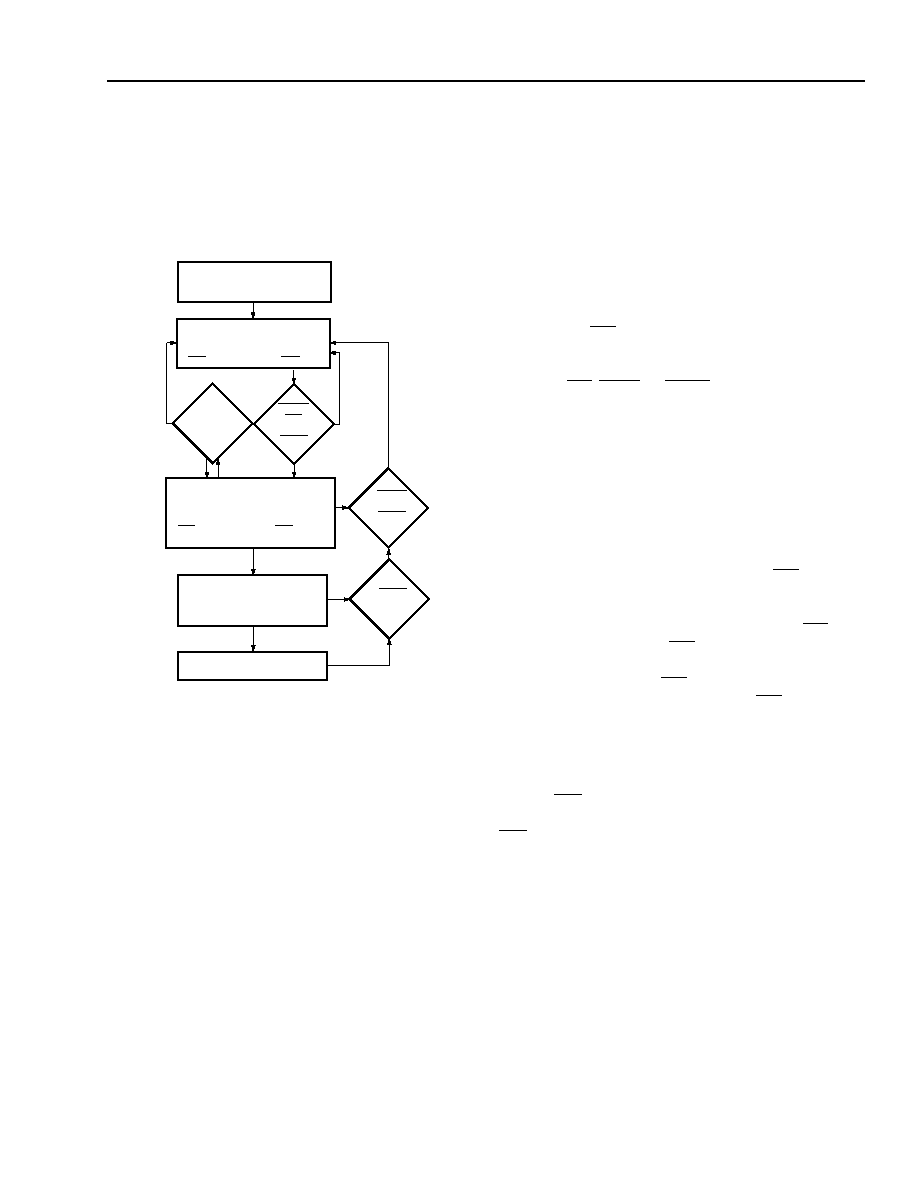
FPGA States of Operation
Prior to becoming operational, the FPGA goes through
a sequence of states, including initialization, congura-
tion, and start-up. Figure 49 outlines these three FPGA
states.
Figure 49. FPGA States of Operation
Initialization
Upon powerup, the device goes through an initialization
process. First, an internal power-on-reset circuit is trig-
gered when power is applied. When VDD reaches the
voltage at which portions of the FPGA begin to operate
(2.5 V to 3 V for the OR3Cxx, 2.2 V to 2.7 V for the
OR3Txxx), the I/Os are congured based on the con-
guration mode, as determined by the mode select
inputs M[2:0]. A time-out delay is initiated when VDD
reaches between 3.0 V and 4.0 V (OR3Cxx) or 2.7 V to
3.0 V (OR3Txxx) to allow the power supply voltage to
stabilize. The INIT and DONE outputs are low. At pow-
erup, if VDD does not rise from 2.0 V to VDD in less than
25 ms, the user should delay conguration by inputting
a low into INIT, PRGM, or RESET until VDD is greater
than the recommended minimum operating voltage
(4.75 V for OR3Cxx commercial devices and 3.0 V for
OR3Txxx devices).
At the end of initialization, the default conguration
option is that the conguration RAM is written to a low
state. This prevents shorts prior to conguration. As a
conguration option, after the rst conguration (i.e., at
reconguration), the user can recongure without
clearing the internal conguration RAM rst. The
active-low, open-drain initialization signal INIT is
released and must be pulled high by an external resis-
tor when initialization is complete. To synchronize the
conguration of multiple FPGAs, one or more INIT pins
should be wire-ANDed. If INIT is held low by one or
more FPGAs or an external device, the FPGA remains
in the initialization state. INIT can be used to signal that
the FPGAs are not yet initialized. After INIT goes high
for two internal clock cycles, the mode lines (M[3:0])
are sampled, and the FPGA enters the conguration
state.
The high during conguration (HDC), low during cong-
uration (LDC), and DONE signals are active outputs in
the FPGA’s initialization and conguration states. HDC,
LDC
, and DONE can be used to provide control of
external logic signals such as reset, bus enable, or
PROM enable during conguration. For parallel master
conguration modes, these signals provide PROM
enable control and allow the data pins to be shared
with user logic signals.
5-4529(F)
– ACTIVE I/O
– RELEASE INTERNAL RESET
– DONE GOES HIGH
START-UP
INITIALIZATION
CONFIGURATION
RESET
OR
PRGM
LOW
PRGM
LOW
– CLEAR CONFIGURATION
– INIT LOW, HDC HIGH, LDC LOW
OPERATION
POWERUP
– POWER-ON TIME DELAY
– M[3:0] MODE IS SELECTED
– CONFIGURATION DATA FRAME
– INIT HIGH, HDC HIGH, LDC LOW
– DOUT ACTIVE
YES
NO
RESET,
INIT,
OR
PRGM
LOW
BIT
ERROR
YES
WRITTEN
MEMORY
Select
devices
have
been
discontinued.
See
Ordering
Information
section
for
product
status.
相關(guān)PDF資料 |
PDF描述 |
|---|---|
| OR3T55-4BA256I | FPGA, 324 CLBS, 40000 GATES, 80 MHz, PBGA256 |
| OR3T55-4BA256 | FPGA, 324 CLBS, 40000 GATES, 80 MHz, PBGA256 |
| OR3T55-4BA352I | FPGA, 324 CLBS, 40000 GATES, 80 MHz, PBGA352 |
| OR3T55-4BA352 | FPGA, 324 CLBS, 40000 GATES, 80 MHz, PBGA352 |
| OR3T80-4BA352I | FPGA, 484 CLBS, 58000 GATES, 80 MHz, PBGA352 |
相關(guān)代理商/技術(shù)參數(shù) |
參數(shù)描述 |
|---|---|
| OR3T80-7PS240I | 制造商:AGERE 制造商全稱:AGERE 功能描述:3C and 3T Field-Programmable Gate Arrays |
| OR3T807S208-DB | 功能描述:FPGA - 現(xiàn)場可編程門陣列 Use LatticeEC RoHS:否 制造商:Altera Corporation 系列:Cyclone V E 柵極數(shù)量: 邏輯塊數(shù)量:943 內(nèi)嵌式塊RAM - EBR:1956 kbit 輸入/輸出端數(shù)量:128 最大工作頻率:800 MHz 工作電源電壓:1.1 V 最大工作溫度:+ 70 C 安裝風(fēng)格:SMD/SMT 封裝 / 箱體:FBGA-256 |
| OR3TP12 | 制造商:AGERE 制造商全稱:AGERE 功能描述:Field-Programmable System Chip (FPSC) Embedded Master/Target PCI Interface |
| OR3TP12-6BA256 | 制造商:未知廠家 制造商全稱:未知廠家 功能描述:User Programmable Special Function ASIC |
| OR3TP126BA256-DB | 功能描述:FPGA - 現(xiàn)場可編程門陣列 2016 LUT 187 I/O RoHS:否 制造商:Altera Corporation 系列:Cyclone V E 柵極數(shù)量: 邏輯塊數(shù)量:943 內(nèi)嵌式塊RAM - EBR:1956 kbit 輸入/輸出端數(shù)量:128 最大工作頻率:800 MHz 工作電源電壓:1.1 V 最大工作溫度:+ 70 C 安裝風(fēng)格:SMD/SMT 封裝 / 箱體:FBGA-256 |
發(fā)布緊急采購,3分鐘左右您將得到回復(fù)。