- 您現(xiàn)在的位置:買賣IC網(wǎng) > PDF目錄224992 > R1230D121H-TL (RICOH COMPANY LTD) SWITCHING REGULATOR, 920 kHz SWITCHING FREQ-MAX, PDSO8 PDF資料下載
參數(shù)資料
| 型號: | R1230D121H-TL |
| 廠商: | RICOH COMPANY LTD |
| 元件分類: | 穩(wěn)壓器 |
| 英文描述: | SWITCHING REGULATOR, 920 kHz SWITCHING FREQ-MAX, PDSO8 |
| 封裝: | 0.9 MM HEIGHT, SON-8 |
| 文件頁數(shù): | 15/20頁 |
| 文件大小: | 401K |
| 代理商: | R1230D121H-TL |
Rev. 1.20
- 4 -
s
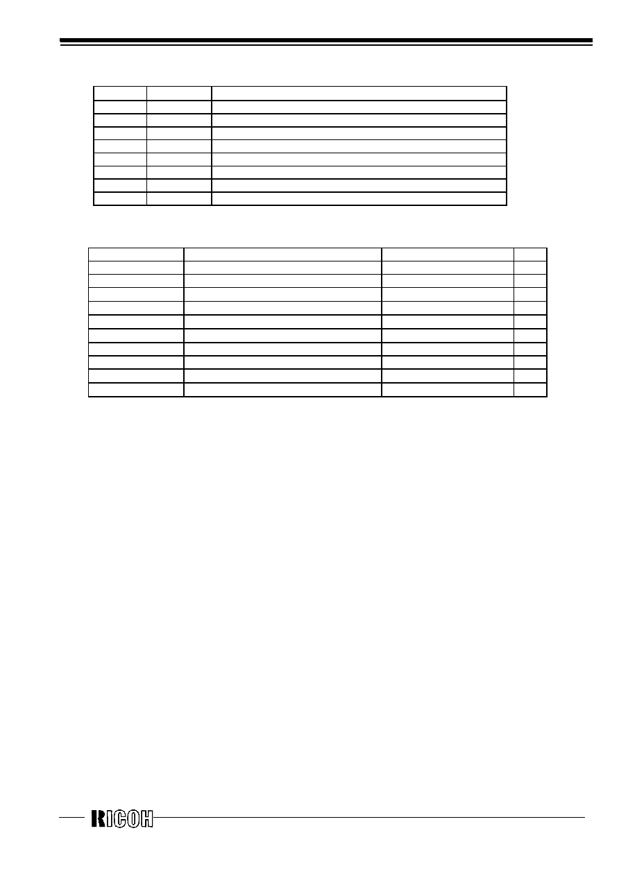
PIN DESCRIPTION
Pin No.
Symbol
Description
1VIN
Voltage Supply Pin
2
PGND
Ground Pin
3VDD
Voltage Supply Pin
4
CE
Chip Enable Pin (active with “H”)
5VOUT/VFB
Output/Feedback Pin
6
MODE
Mode changer Pin (PWM mode at “L”, VFM mode at “H”.)
7
AGND
Ground Pin
8Lx
Lx Pin
s
ABSOLUTE MAXIMUM RATINGS
(AGND=PGND=0V)
Symbol
Item
Rating
Unit
VIN
VIN Supply Voltage
6.5
V
VDD
VDD Pin Voltage
6.5
V
VLX
Lx Pin Voltage
-0.3
VIN+0.3
V
VCE
CE Pin Input Voltage
-0.3
VIN+0.3
V
VMODE
MODE Pin Input Voltage
-0.3
VIN+0.3
V
VFB
VFB Pin Input Voltage
-0.3
VIN+0.3
V
ILX
LX Pin Output Current
-0.8
A
PD
Power Dissipation
300
mW
Topt
Operating Temperature Range
-40
+85
°C
Tstg
Storage Temperature Range
-55
+125
°C
相關(guān)PDF資料 |
PDF描述 |
|---|---|
| R1230D161H-TL | SWITCHING REGULATOR, 920 kHz SWITCHING FREQ-MAX, PDSO8 |
| R1230D201G-TL | SWITCHING REGULATOR, 575 kHz SWITCHING FREQ-MAX, PDSO8 |
| R1230D281E-TL | SWITCHING REGULATOR, 575 kHz SWITCHING FREQ-MAX, PDSO8 |
| R1242S001F-E2-FE | SWITCHING REGULATOR, 550 kHz SWITCHING FREQ-MAX, PDSO8 |
| R125.461.171 | PANEL MOUNT, FEMALE, SMA CONNECTOR, RECEPTACLE |
相關(guān)代理商/技術(shù)參數(shù) |
參數(shù)描述 |
|---|---|
| R1230D131A-TL | 制造商:未知廠家 制造商全稱:未知廠家 功能描述:SMPS Controller |
| R1230D131A-TR | 制造商:未知廠家 制造商全稱:未知廠家 功能描述:SMPS Controller |
| R1230D131B-TL | 制造商:未知廠家 制造商全稱:未知廠家 功能描述:SMPS Controller |
| R1230D131B-TR | 制造商:未知廠家 制造商全稱:未知廠家 功能描述:SMPS Controller |
| R1230D141A-TL | 制造商:未知廠家 制造商全稱:未知廠家 功能描述:SMPS Controller |
發(fā)布緊急采購,3分鐘左右您將得到回復(fù)。