- 您現在的位置:買賣IC網 > PDF目錄299576 > OR3T165-4PS240I FPGA, 1024 CLBS, 120000 GATES, PQFP240 PDF資料下載
參數資料
| 型號: | OR3T165-4PS240I |
| 元件分類: | FPGA |
| 英文描述: | FPGA, 1024 CLBS, 120000 GATES, PQFP240 |
| 封裝: | SQFP-240 |
| 文件頁數: | 202/210頁 |
| 文件大?。?/td> | 2138K |
| 代理商: | OR3T165-4PS240I |
第1頁第2頁第3頁第4頁第5頁第6頁第7頁第8頁第9頁第10頁第11頁第12頁第13頁第14頁第15頁第16頁第17頁第18頁第19頁第20頁第21頁第22頁第23頁第24頁第25頁第26頁第27頁第28頁第29頁第30頁第31頁第32頁第33頁第34頁第35頁第36頁第37頁第38頁第39頁第40頁第41頁第42頁第43頁第44頁第45頁第46頁第47頁第48頁第49頁第50頁第51頁第52頁第53頁第54頁第55頁第56頁第57頁第58頁第59頁第60頁第61頁第62頁第63頁第64頁第65頁第66頁第67頁第68頁第69頁第70頁第71頁第72頁第73頁第74頁第75頁第76頁第77頁第78頁第79頁第80頁第81頁第82頁第83頁第84頁第85頁第86頁第87頁第88頁第89頁第90頁第91頁第92頁第93頁第94頁第95頁第96頁第97頁第98頁第99頁第100頁第101頁第102頁第103頁第104頁第105頁第106頁第107頁第108頁第109頁第110頁第111頁第112頁第113頁第114頁第115頁第116頁第117頁第118頁第119頁第120頁第121頁第122頁第123頁第124頁第125頁第126頁第127頁第128頁第129頁第130頁第131頁第132頁第133頁第134頁第135頁第136頁第137頁第138頁第139頁第140頁第141頁第142頁第143頁第144頁第145頁第146頁第147頁第148頁第149頁第150頁第151頁第152頁第153頁第154頁第155頁第156頁第157頁第158頁第159頁第160頁第161頁第162頁第163頁第164頁第165頁第166頁第167頁第168頁第169頁第170頁第171頁第172頁第173頁第174頁第175頁第176頁第177頁第178頁第179頁第180頁第181頁第182頁第183頁第184頁第185頁第186頁第187頁第188頁第189頁第190頁第191頁第192頁第193頁第194頁第195頁第196頁第197頁第198頁第199頁第200頁第201頁當前第202頁第203頁第204頁第205頁第206頁第207頁第208頁第209頁第210頁
Lucent Technologies Inc.
91
Preliminary Data Sheet, Rev. 1
September 1998
ORCA Series 3 FPGAs
FPGA Configuration Modes (continued)
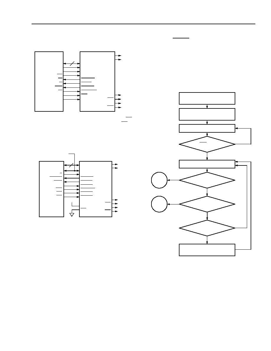
Note: FPGA shown as a memory-mapped peripheral using CS0 and
CS1. Other decoding schemes are possible using CS0 and/or
CS1.
Figure 57.
PowerPC/MPI Configuration Schematic
Note: FPGA shown as only system peripheral with fixed chip select
signals. For multiperipheral systems, address decoding and/
or latching can be used to implement chip selects.
Figure 58.
i960/MPI Configuration Schematic
Configuration readback can also be performed via the
MPI
when it is in user mode. The MPI is enabled in
user mode by setting the MP_USER bit to 1 in the con-
figuration control register prior to the start of configura-
tion or through a configuration option. To perform
readback, the host processor writes the 14-bit read-
back start address to the readback address registers
and sets the RD_CFG bit to 0 in the configuration con-
trol register. Readback data is returned 8 bits at a time
to the readback data register and is valid when the
DATA_RDY bit of the status register is 1. A flow chart of
the MPI readback operation is shown in Figure 60. The
RD_DATA pin used for dedicated FPGA readback is
invalid during MPI readback.
5-5763(F)
Figure 59. Configuration Through MPI
DOUT
CCLK
D[7:0]
A[4:0]
MPI_CLK
MPI_RW
MPI_ACK
MPI_BI
MPI_IRQ
MPI_STRB
CS0
CS1
HDC
LDC
D[7:0]
A[27:31]
CLKOUT
RD/WR
TA
BI
IRQx
TS
A26
A25
TO DAISY-
CHAINED
DEVICES
POWERPC
ORCA
8
FPGA
SERIES 3
DONE
INIT
DOUT
CCLK
D[7:0]
MPI_CLK
MPI_RW
MPI_ACK
MPI_IRQ
MPI_ALE
MPI_BE1
HDC
LDC
TO DAISY-
CHAINED
DEVICES
ORCA
8
FPGA
SERIES 3
DONE
INIT
AD[7:0]
CLKIN
W/R
RDYRCV
XINTx
ALE
BE1
i960
CS1
CS0
i960 SYSTEM CLOCK
VDD
MPI_BE0
BE0
MPI_STRB
ADS
POWER ON WITH
WRITE CONFIGURATION
READ STATUS REGISTER
INIT = 1?
NO
READ STATUS REGISTER
BIT STREAM ERROR?
DATA_RDY = 1?
WRITE DATA TO
DONE = 1?
DONE
ERROR
YES
NO
YES
NO
VALID M[3:0]
CONTROL REGISTER BITS
CONFIGURATION DATA REG
5-5761(F)
5-5762(F)
相關PDF資料 |
PDF描述 |
|---|---|
| OR3T165-4PS240 | FPGA, 1024 CLBS, 120000 GATES, PQFP240 |
| OR3T165-5B432 | FPGA, 1024 CLBS, 120000 GATES, PBGA432 |
| OR3T165-5B600 | FPGA, 1024 CLBS, 120000 GATES, PBGA600 |
| OR3T165-5BA352I | FPGA, 1024 CLBS, 120000 GATES, PBGA352 |
| OR3T165-5BA352 | FPGA, 1024 CLBS, 120000 GATES, PBGA352 |
相關代理商/技術參數 |
參數描述 |
|---|---|
| OR3T20 | 制造商:AGERE 制造商全稱:AGERE 功能描述:3C and 3T Field-Programmable Gate Arrays |
| OR3T20-4BA256I | 制造商:未知廠家 制造商全稱:未知廠家 功能描述:Field Programmable Gate Array (FPGA) |
| OR3T20-4S208I | 制造商:未知廠家 制造商全稱:未知廠家 功能描述:Field Programmable Gate Array (FPGA) |
| OR3T20-4S240I | 制造商:未知廠家 制造商全稱:未知廠家 功能描述:Field Programmable Gate Array (FPGA) |
| OR3T20-5BA256 | 制造商:AGERE 制造商全稱:AGERE 功能描述:3C and 3T Field-Programmable Gate Arrays |
發(fā)布緊急采購,3分鐘左右您將得到回復。