- 您現在的位置:買賣IC網 > PDF目錄299576 > OR3T165-4BA352I FPGA, 1024 CLBS, 120000 GATES, PBGA352 PDF資料下載
參數資料
| 型號: | OR3T165-4BA352I |
| 元件分類: | FPGA |
| 英文描述: | FPGA, 1024 CLBS, 120000 GATES, PBGA352 |
| 封裝: | PLASTIC, BGA-352 |
| 文件頁數: | 188/210頁 |
| 文件大小: | 2138K |
| 代理商: | OR3T165-4BA352I |
第1頁第2頁第3頁第4頁第5頁第6頁第7頁第8頁第9頁第10頁第11頁第12頁第13頁第14頁第15頁第16頁第17頁第18頁第19頁第20頁第21頁第22頁第23頁第24頁第25頁第26頁第27頁第28頁第29頁第30頁第31頁第32頁第33頁第34頁第35頁第36頁第37頁第38頁第39頁第40頁第41頁第42頁第43頁第44頁第45頁第46頁第47頁第48頁第49頁第50頁第51頁第52頁第53頁第54頁第55頁第56頁第57頁第58頁第59頁第60頁第61頁第62頁第63頁第64頁第65頁第66頁第67頁第68頁第69頁第70頁第71頁第72頁第73頁第74頁第75頁第76頁第77頁第78頁第79頁第80頁第81頁第82頁第83頁第84頁第85頁第86頁第87頁第88頁第89頁第90頁第91頁第92頁第93頁第94頁第95頁第96頁第97頁第98頁第99頁第100頁第101頁第102頁第103頁第104頁第105頁第106頁第107頁第108頁第109頁第110頁第111頁第112頁第113頁第114頁第115頁第116頁第117頁第118頁第119頁第120頁第121頁第122頁第123頁第124頁第125頁第126頁第127頁第128頁第129頁第130頁第131頁第132頁第133頁第134頁第135頁第136頁第137頁第138頁第139頁第140頁第141頁第142頁第143頁第144頁第145頁第146頁第147頁第148頁第149頁第150頁第151頁第152頁第153頁第154頁第155頁第156頁第157頁第158頁第159頁第160頁第161頁第162頁第163頁第164頁第165頁第166頁第167頁第168頁第169頁第170頁第171頁第172頁第173頁第174頁第175頁第176頁第177頁第178頁第179頁第180頁第181頁第182頁第183頁第184頁第185頁第186頁第187頁當前第188頁第189頁第190頁第191頁第192頁第193頁第194頁第195頁第196頁第197頁第198頁第199頁第200頁第201頁第202頁第203頁第204頁第205頁第206頁第207頁第208頁第209頁第210頁
Preliminary Data Sheet, Rev. 1
September 1998
ORCA Series 3 FPGAs
Lucent Technologies Inc.
79
Programmable Clock Manager (PCM):
Advance Information (continued)
PCM Applications
The applications discussed below are only a small
sampling of the possible uses for the PCM. Check the
Lucent Technologies
ORCA FPGA Internet web site
(listed at the end of this data sheet) for additional appli-
cation notes.
Clock Phase Adjustment
The PCM may be used to adjust the phase of the input
clock. The result is an output clock which has its active
edge either preceding or following the active edge of
the input clock. Clock phase adjustment is accom-
plished in DLL mode by delaying the clock. This is dis-
cussed in the Delay-Locked Loop (DLL) Mode section.
Examples of using the delayed clock as an early or late
phase-adjusted clock are outlined in the following para-
graphs.
An output clock that precedes the input clock can be
used to compensate for clock delay that is largely due
to excessive loading. The preceding output clock is
really not early relative to the input clock, but is delayed
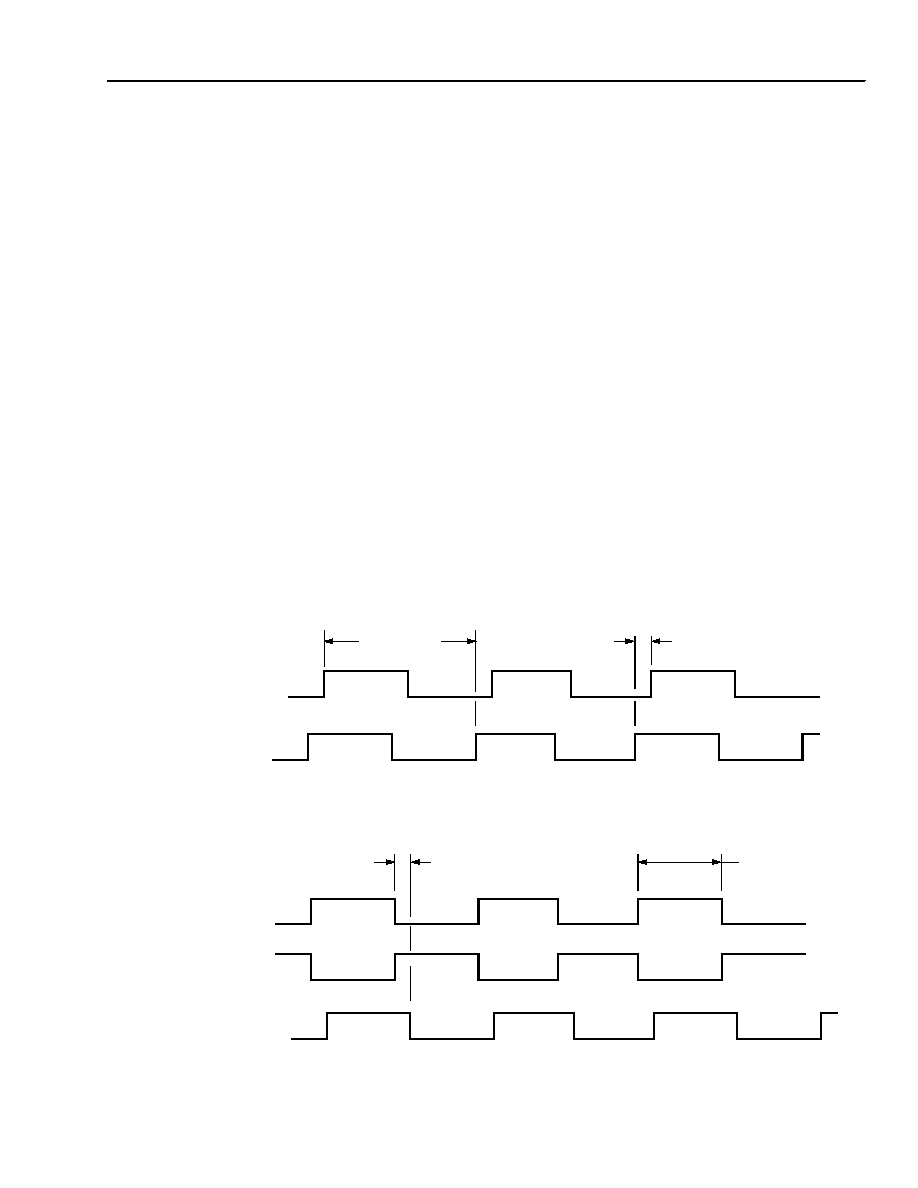
almost a full cycle. This is shown in Figure 48A. The
amount of delay that is being compensated for, plus
clock setup time and some margin, is the amount less
than one full clock cycle that the output clock is delayed
from the input clock.
In some systems, it is desirable to operate logic from
several clocks that operate at different phases. This
technique is often used in microprocessor-based sys-
tems to transfer and process data synchronously
between functional areas, but without incurring exces-
sive delays. Figure 48B shows an input clock and an
output clock operating 180° out of phase. It also shows
a version of the input clock that was shifted approxi-
mately 180° using logic gates to create an inverter.
Note that the inverted clock is really shifted more than
180° due to the propagation delay of the inverter. The
PCM
output clock does not suffer from this delay. Addi-
tionally, the 180° shifted PCM output could be shifted
by some smaller amount to effect an early 180° shifted
clock that also accounts for loading effects.
In terms of degrees of phase shift, the phase of a clock
is adjustable in DLL mode with resolution relative to the
delay increment (see Table 27):
Phase Adjustment = (Delay)* 11.25,
Delay < 16
Phase Adjustment = ((Delay)* 11.25) – 360,
Delay > 16
Figure 48. Clock Phase Adjustment Using the PCM
INPUT CLOCK
OUTPUT CLOCK
INPUT CLOCK
PCM OUTPUT CLOCK
INVERTED INPUT CLOCK
A. Generating an Early Clock
B. Multiphase Clock Generation Using the DLL
UNINTENDED PHASE
SHIFT DUE TO
INVERTER DELAY
DLL DELAY
CLOCK DELAY AND SETUP
BEING COMPENSATED
5-5979(F)
相關PDF資料 |
PDF描述 |
|---|---|
| OR3T165-4BA352 | FPGA, 1024 CLBS, 120000 GATES, PBGA352 |
| OR3T165-4BC432I | FPGA, 1024 CLBS, 120000 GATES, PBGA432 |
| OR3T165-4BC600I | FPGA, 1024 CLBS, 120000 GATES, PBGA600 |
| OR3T165-4PS208I | FPGA, 1024 CLBS, 120000 GATES, PQFP208 |
| OR3T165-4PS208 | FPGA, 1024 CLBS, 120000 GATES, PQFP208 |
相關代理商/技術參數 |
參數描述 |
|---|---|
| OR3T20 | 制造商:AGERE 制造商全稱:AGERE 功能描述:3C and 3T Field-Programmable Gate Arrays |
| OR3T20-4BA256I | 制造商:未知廠家 制造商全稱:未知廠家 功能描述:Field Programmable Gate Array (FPGA) |
| OR3T20-4S208I | 制造商:未知廠家 制造商全稱:未知廠家 功能描述:Field Programmable Gate Array (FPGA) |
| OR3T20-4S240I | 制造商:未知廠家 制造商全稱:未知廠家 功能描述:Field Programmable Gate Array (FPGA) |
| OR3T20-5BA256 | 制造商:AGERE 制造商全稱:AGERE 功能描述:3C and 3T Field-Programmable Gate Arrays |
發(fā)布緊急采購,3分鐘左右您將得到回復。