- 您現(xiàn)在的位置:買賣IC網(wǎng) > PDF目錄299576 > OR3T125-6B432 FPGA, 784 CLBS, 92000 GATES, PBGA432 PDF資料下載
參數(shù)資料
| 型號(hào): | OR3T125-6B432 |
| 元件分類: | FPGA |
| 英文描述: | FPGA, 784 CLBS, 92000 GATES, PBGA432 |
| 封裝: | BGA-432 |
| 文件頁(yè)數(shù): | 179/210頁(yè) |
| 文件大?。?/td> | 2138K |
| 代理商: | OR3T125-6B432 |
第1頁(yè)第2頁(yè)第3頁(yè)第4頁(yè)第5頁(yè)第6頁(yè)第7頁(yè)第8頁(yè)第9頁(yè)第10頁(yè)第11頁(yè)第12頁(yè)第13頁(yè)第14頁(yè)第15頁(yè)第16頁(yè)第17頁(yè)第18頁(yè)第19頁(yè)第20頁(yè)第21頁(yè)第22頁(yè)第23頁(yè)第24頁(yè)第25頁(yè)第26頁(yè)第27頁(yè)第28頁(yè)第29頁(yè)第30頁(yè)第31頁(yè)第32頁(yè)第33頁(yè)第34頁(yè)第35頁(yè)第36頁(yè)第37頁(yè)第38頁(yè)第39頁(yè)第40頁(yè)第41頁(yè)第42頁(yè)第43頁(yè)第44頁(yè)第45頁(yè)第46頁(yè)第47頁(yè)第48頁(yè)第49頁(yè)第50頁(yè)第51頁(yè)第52頁(yè)第53頁(yè)第54頁(yè)第55頁(yè)第56頁(yè)第57頁(yè)第58頁(yè)第59頁(yè)第60頁(yè)第61頁(yè)第62頁(yè)第63頁(yè)第64頁(yè)第65頁(yè)第66頁(yè)第67頁(yè)第68頁(yè)第69頁(yè)第70頁(yè)第71頁(yè)第72頁(yè)第73頁(yè)第74頁(yè)第75頁(yè)第76頁(yè)第77頁(yè)第78頁(yè)第79頁(yè)第80頁(yè)第81頁(yè)第82頁(yè)第83頁(yè)第84頁(yè)第85頁(yè)第86頁(yè)第87頁(yè)第88頁(yè)第89頁(yè)第90頁(yè)第91頁(yè)第92頁(yè)第93頁(yè)第94頁(yè)第95頁(yè)第96頁(yè)第97頁(yè)第98頁(yè)第99頁(yè)第100頁(yè)第101頁(yè)第102頁(yè)第103頁(yè)第104頁(yè)第105頁(yè)第106頁(yè)第107頁(yè)第108頁(yè)第109頁(yè)第110頁(yè)第111頁(yè)第112頁(yè)第113頁(yè)第114頁(yè)第115頁(yè)第116頁(yè)第117頁(yè)第118頁(yè)第119頁(yè)第120頁(yè)第121頁(yè)第122頁(yè)第123頁(yè)第124頁(yè)第125頁(yè)第126頁(yè)第127頁(yè)第128頁(yè)第129頁(yè)第130頁(yè)第131頁(yè)第132頁(yè)第133頁(yè)第134頁(yè)第135頁(yè)第136頁(yè)第137頁(yè)第138頁(yè)第139頁(yè)第140頁(yè)第141頁(yè)第142頁(yè)第143頁(yè)第144頁(yè)第145頁(yè)第146頁(yè)第147頁(yè)第148頁(yè)第149頁(yè)第150頁(yè)第151頁(yè)第152頁(yè)第153頁(yè)第154頁(yè)第155頁(yè)第156頁(yè)第157頁(yè)第158頁(yè)第159頁(yè)第160頁(yè)第161頁(yè)第162頁(yè)第163頁(yè)第164頁(yè)第165頁(yè)第166頁(yè)第167頁(yè)第168頁(yè)第169頁(yè)第170頁(yè)第171頁(yè)第172頁(yè)第173頁(yè)第174頁(yè)第175頁(yè)第176頁(yè)第177頁(yè)第178頁(yè)當(dāng)前第179頁(yè)第180頁(yè)第181頁(yè)第182頁(yè)第183頁(yè)第184頁(yè)第185頁(yè)第186頁(yè)第187頁(yè)第188頁(yè)第189頁(yè)第190頁(yè)第191頁(yè)第192頁(yè)第193頁(yè)第194頁(yè)第195頁(yè)第196頁(yè)第197頁(yè)第198頁(yè)第199頁(yè)第200頁(yè)第201頁(yè)第202頁(yè)第203頁(yè)第204頁(yè)第205頁(yè)第206頁(yè)第207頁(yè)第208頁(yè)第209頁(yè)第210頁(yè)
Preliminary Data Sheet, Rev. 1
ORCA Series 3 FPGAs
September 1998
70
Lucent Technologies Inc.
Programmable Clock Manager (PCM): Advance Information (continued)
PCM Registers
The PCM contains eight user-programmable registers used for configuring the PCM’s functionality. Table 26 shows
the mapping of the registers and their functions. See Figure 46 for more information on the location of PCM ele-
ments that are discussed in the table. The PCM registers are referenced in the discussions that follow. Detailed
explanations of all register bits are supplied following the functional description of the PCM.
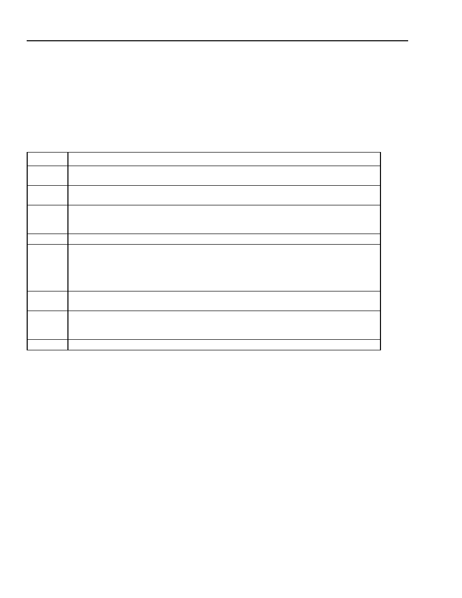
Table 26. PCM Registers
Address
Function
0
Divider 0 Programming. Programmable divider, DIV0, value and DIV0 reset bit. DIV0 can
divide the input clock to the PCM or can be bypassed.
1
Divider 1 Programming. Programmable divider, DIV1, value and DIV1 reset bit. DIV1 can
divide the feedback clock input to the PCM or can be bypassed. Valid only in PLL mode.
2
Divider 2 Programming. Programmable divider, DIV2, value and DIV2 reset bit. DIV2 can
divide the output of the tapped delay line or can be bypassed and is only valid for the
ExpressCLK
output.
3
DLL 2x Duty-Cycle Programming. DLL mode clock doubler (2x) duty-cycle selection.
4
DLL 1x Duty-Cycle Programming. Depending on the settings in other registers, this regis-
ter is for:
a. PLL mode phase/delay selection;
b. DLL mode 1x duty cycle selection; and
c. DLL mode programmable delay.
5
Mode Programming. DLL/PLL mode selection, DLL 1x/2x clock selection, phase detector
feedback selection.
6
Clock Source Status/Output Clock Selection Programming. Input clock selection, feed-
back clock selection, ExpressCLK output source selection, system clock output source
selection.
7
PCM Control Programming. PCM power, reset, and configuration control.
相關(guān)PDF資料 |
PDF描述 |
|---|---|
| OR3T125-6B600 | FPGA, 784 CLBS, 92000 GATES, PBGA600 |
| OR3T165-4B432 | FPGA, 1024 CLBS, 120000 GATES, PBGA432 |
| OR3T165-4B600 | FPGA, 1024 CLBS, 120000 GATES, PBGA600 |
| OR3T165-4BA352I | FPGA, 1024 CLBS, 120000 GATES, PBGA352 |
| OR3T165-4BA352 | FPGA, 1024 CLBS, 120000 GATES, PBGA352 |
相關(guān)代理商/技術(shù)參數(shù) |
參數(shù)描述 |
|---|---|
| OR3T125-6BA352 | 制造商:AGERE 制造商全稱:AGERE 功能描述:3C and 3T Field-Programmable Gate Arrays |
| OR3T1256BA352-DB | 功能描述:FPGA - 現(xiàn)場(chǎng)可編程門陣列 6272 LUT 342 I/O RoHS:否 制造商:Altera Corporation 系列:Cyclone V E 柵極數(shù)量: 邏輯塊數(shù)量:943 內(nèi)嵌式塊RAM - EBR:1956 kbit 輸入/輸出端數(shù)量:128 最大工作頻率:800 MHz 工作電源電壓:1.1 V 最大工作溫度:+ 70 C 安裝風(fēng)格:SMD/SMT 封裝 / 箱體:FBGA-256 |
| OR3T125-6BA352I | 制造商:AGERE 制造商全稱:AGERE 功能描述:3C and 3T Field-Programmable Gate Arrays |
| OR3T1256BA352I-DB | 功能描述:FPGA - 現(xiàn)場(chǎng)可編程門陣列 6272 LUT 342 I/O RoHS:否 制造商:Altera Corporation 系列:Cyclone V E 柵極數(shù)量: 邏輯塊數(shù)量:943 內(nèi)嵌式塊RAM - EBR:1956 kbit 輸入/輸出端數(shù)量:128 最大工作頻率:800 MHz 工作電源電壓:1.1 V 最大工作溫度:+ 70 C 安裝風(fēng)格:SMD/SMT 封裝 / 箱體:FBGA-256 |
| OR3T125-6BC432 | 制造商:AGERE 制造商全稱:AGERE 功能描述:3C and 3T Field-Programmable Gate Arrays |
發(fā)布緊急采購(gòu),3分鐘左右您將得到回復(fù)。