- 您現(xiàn)在的位置:買(mǎi)賣(mài)IC網(wǎng) > PDF目錄299576 > OR3C80-5B432 FPGA, 484 CLBS, 58000 GATES, PBGA432 PDF資料下載
參數(shù)資料
| 型號(hào): | OR3C80-5B432 |
| 元件分類(lèi): | FPGA |
| 英文描述: | FPGA, 484 CLBS, 58000 GATES, PBGA432 |
| 封裝: | BGA-432 |
| 文件頁(yè)數(shù): | 157/210頁(yè) |
| 文件大小: | 2138K |
| 代理商: | OR3C80-5B432 |
第1頁(yè)第2頁(yè)第3頁(yè)第4頁(yè)第5頁(yè)第6頁(yè)第7頁(yè)第8頁(yè)第9頁(yè)第10頁(yè)第11頁(yè)第12頁(yè)第13頁(yè)第14頁(yè)第15頁(yè)第16頁(yè)第17頁(yè)第18頁(yè)第19頁(yè)第20頁(yè)第21頁(yè)第22頁(yè)第23頁(yè)第24頁(yè)第25頁(yè)第26頁(yè)第27頁(yè)第28頁(yè)第29頁(yè)第30頁(yè)第31頁(yè)第32頁(yè)第33頁(yè)第34頁(yè)第35頁(yè)第36頁(yè)第37頁(yè)第38頁(yè)第39頁(yè)第40頁(yè)第41頁(yè)第42頁(yè)第43頁(yè)第44頁(yè)第45頁(yè)第46頁(yè)第47頁(yè)第48頁(yè)第49頁(yè)第50頁(yè)第51頁(yè)第52頁(yè)第53頁(yè)第54頁(yè)第55頁(yè)第56頁(yè)第57頁(yè)第58頁(yè)第59頁(yè)第60頁(yè)第61頁(yè)第62頁(yè)第63頁(yè)第64頁(yè)第65頁(yè)第66頁(yè)第67頁(yè)第68頁(yè)第69頁(yè)第70頁(yè)第71頁(yè)第72頁(yè)第73頁(yè)第74頁(yè)第75頁(yè)第76頁(yè)第77頁(yè)第78頁(yè)第79頁(yè)第80頁(yè)第81頁(yè)第82頁(yè)第83頁(yè)第84頁(yè)第85頁(yè)第86頁(yè)第87頁(yè)第88頁(yè)第89頁(yè)第90頁(yè)第91頁(yè)第92頁(yè)第93頁(yè)第94頁(yè)第95頁(yè)第96頁(yè)第97頁(yè)第98頁(yè)第99頁(yè)第100頁(yè)第101頁(yè)第102頁(yè)第103頁(yè)第104頁(yè)第105頁(yè)第106頁(yè)第107頁(yè)第108頁(yè)第109頁(yè)第110頁(yè)第111頁(yè)第112頁(yè)第113頁(yè)第114頁(yè)第115頁(yè)第116頁(yè)第117頁(yè)第118頁(yè)第119頁(yè)第120頁(yè)第121頁(yè)第122頁(yè)第123頁(yè)第124頁(yè)第125頁(yè)第126頁(yè)第127頁(yè)第128頁(yè)第129頁(yè)第130頁(yè)第131頁(yè)第132頁(yè)第133頁(yè)第134頁(yè)第135頁(yè)第136頁(yè)第137頁(yè)第138頁(yè)第139頁(yè)第140頁(yè)第141頁(yè)第142頁(yè)第143頁(yè)第144頁(yè)第145頁(yè)第146頁(yè)第147頁(yè)第148頁(yè)第149頁(yè)第150頁(yè)第151頁(yè)第152頁(yè)第153頁(yè)第154頁(yè)第155頁(yè)第156頁(yè)當(dāng)前第157頁(yè)第158頁(yè)第159頁(yè)第160頁(yè)第161頁(yè)第162頁(yè)第163頁(yè)第164頁(yè)第165頁(yè)第166頁(yè)第167頁(yè)第168頁(yè)第169頁(yè)第170頁(yè)第171頁(yè)第172頁(yè)第173頁(yè)第174頁(yè)第175頁(yè)第176頁(yè)第177頁(yè)第178頁(yè)第179頁(yè)第180頁(yè)第181頁(yè)第182頁(yè)第183頁(yè)第184頁(yè)第185頁(yè)第186頁(yè)第187頁(yè)第188頁(yè)第189頁(yè)第190頁(yè)第191頁(yè)第192頁(yè)第193頁(yè)第194頁(yè)第195頁(yè)第196頁(yè)第197頁(yè)第198頁(yè)第199頁(yè)第200頁(yè)第201頁(yè)第202頁(yè)第203頁(yè)第204頁(yè)第205頁(yè)第206頁(yè)第207頁(yè)第208頁(yè)第209頁(yè)第210頁(yè)
50
Lucent Technologies Inc.
Preliminary Data Sheet, Rev. 1
ORCA Series 3 FPGAs
September 1998
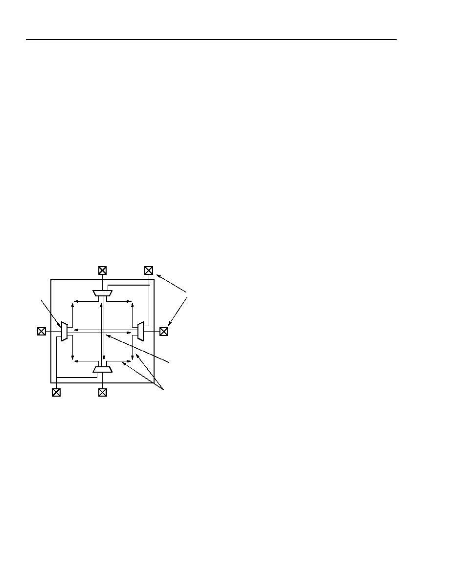
Clock Distribution Network (continued)
ExpressCLK Inputs
There are four dedicated ExpressCLK pads on each
Series 3 device: one in the middle of each side. Two
other user I/O pads can also be used as corner
ExpressCLK
inputs, one on the lower-left corner, and
one on the upper-right corner. The corner ExpressCLK
pads feed the ExpressCLK to the two sides of the array
that are adjacent to that corner, always driving the
same signal in both directions. The ExpressCLK route
from the middle pad and from the corner pad associ-
ated with that side are multiplexed and can be glitch-
lessly stopped/started under user control using the
StopCLK
feature of the CLKCNTRL function block
(described under Special Function Blocks) on that side.
The ExpressCLK output of the programmable clock
manager (PCM) is programmably connected to the cor-
ner ExpressCLK routes. PCM blocks are found in the
same corners as the corner ExpressCLK signals and
are described in the Special Function Blocks section.
The ExpressCLK structure is shown in Figure 34 (PCM
blocks are not shown).
Note: All multiplexers are set during configuration.
Figure 34. ExpressCLK and Fast Clock Distribution
Selecting Clock Input Pins
Any user I/O pin on an
ORCA FPGA can be used as a
fast, low-skew system clock input. Since the four dedi-
cated ExpressCLK inputs can only be used to distribute
global signals into the FPGA, these pins should be
selected first as clock pins. Within the interquad region
of the device, these clocks sourced by the ExpressCLK
inputs are called Fast Clocks. Choosing the next clock
pin is completely arbitrary, but using a pin that is near
the center of an edge of the device will provide the low-
est skew system clock network. The pin-to-pin timing
numbers in the Timing Characteristics section assume
that the clock pin is in one of the PICs at the center of
any side of the device next to an ExpressCLK pad. For
actual timing characteristics for a given clock pin, use
the timing analyzer results from
ORCA Foundry.
To select subsequent clock pins, certain rules should
be followed. As discussed in the Programmable Input/
Output Cells section, PICs are grouped into adjacent
pairs. Each of these pairs contains eight I/Os, but only
one of the eight I/Os in a PIC pair can be routed directly
onto a system clock spine. Therefore, to achieve top
performance, the next clock input chosen should not be
one of the pins from a PIC pair previously used for a
clock input. If it is necessary to have a second input in
the same PIC pair route onto global system clock rout-
ing, the input can be routed to a free clock spine using
the PIC switching segment (pSW) connections to the
clock spine network at some small sacrifice in speed.
Alternatively, if global distribution of the secondary
clock is not required, the signal can be routed on long
lines (xL) and input to the PFU clock input without
using a clock spine.
Another rule for choosing clock pins has to do with the
alternating nature of clock spine connections to the xL
and pxL routing segments. Starting at the left side of
the device, the first vertical clock spine from the top
connects to hxL[0] (horizontal xL[0]), and the first verti-
cal clock spine from the bottom connects to hxL[5] in all
PLC rows. The next vertical clock spine from the top
connects to hxL[1], and the next one from the bottom
connects to hxL[6]. This progression continues across
the device, and after a spine connects to hxL[9], the
next spine connects to hxL[0] again. Similar connec-
tions are made from horizontal clock spines to vxL (ver-
tical xL) lines from the top to the bottom of the device.
Because the
ORCA Series 3 clock routing only
requires the use of an xL line in every other row or col-
umn, even two inputs chosen 20 PLCs apart on the
same xL line will not conflict, but it is always better to
avoid these choices, if possible. The Fast Clock spines
in the interquad routing region also connect to xL[8]
and xL[9] for each set of xL lines, so it is better to avoid
user I/Os that connect to xL[8] or xL[9] when a Fast
Clock is used that might share one of these connec-
tions. Another reason to use the Fast Clock spines is
that since they use only the xL[9:8] lines, they will not
conflict with internal data buses which typically use
xL[7:0]. For more details on clock selection, refer to
application notes on clock distribution in
ORCA Series
3 devices.
ExpressCLKs TO PIOs
FAST CLOCKS
ExpressCLK PADS
CLKCNTRL
BLOCK
5-5802(F)
相關(guān)PDF資料 |
PDF描述 |
|---|---|
| OR3C80-5B600 | FPGA, 484 CLBS, 58000 GATES, PBGA600 |
| OR3T125-4B432 | FPGA, 784 CLBS, 92000 GATES, PBGA432 |
| OR3T125-4B600 | FPGA, 784 CLBS, 92000 GATES, PBGA600 |
| OR3T125-4BA352I | FPGA, 784 CLBS, 92000 GATES, PBGA352 |
| OR3T125-4BA352 | FPGA, 784 CLBS, 92000 GATES, PBGA352 |
相關(guān)代理商/技術(shù)參數(shù) |
參數(shù)描述 |
|---|---|
| OR3C80-5BA352 | 制造商:AGERE 制造商全稱(chēng):AGERE 功能描述:3C and 3T Field-Programmable Gate Arrays |
| OR3C805BA352-DB | 功能描述:FPGA - 現(xiàn)場(chǎng)可編程門(mén)陣列 3872 LUT 356 I/O RoHS:否 制造商:Altera Corporation 系列:Cyclone V E 柵極數(shù)量: 邏輯塊數(shù)量:943 內(nèi)嵌式塊RAM - EBR:1956 kbit 輸入/輸出端數(shù)量:128 最大工作頻率:800 MHz 工作電源電壓:1.1 V 最大工作溫度:+ 70 C 安裝風(fēng)格:SMD/SMT 封裝 / 箱體:FBGA-256 |
| OR3C80-5BA352I | 制造商:AGERE 制造商全稱(chēng):AGERE 功能描述:3C and 3T Field-Programmable Gate Arrays |
| OR3C80-5BC432 | 制造商:AGERE 制造商全稱(chēng):AGERE 功能描述:3C and 3T Field-Programmable Gate Arrays |
| OR3C80-5BC432I | 制造商:AGERE 制造商全稱(chēng):AGERE 功能描述:3C and 3T Field-Programmable Gate Arrays |
發(fā)布緊急采購(gòu),3分鐘左右您將得到回復(fù)。