- 您現(xiàn)在的位置:買(mǎi)賣(mài)IC網(wǎng) > PDF目錄359273 > NJU26175 (New Japan Radio Co., Ltd.) NJU26100 Series Hardware Specification PDF資料下載
參數(shù)資料
| 型號(hào): | NJU26175 |
| 廠商: | New Japan Radio Co., Ltd. |
| 英文描述: | NJU26100 Series Hardware Specification |
| 中文描述: | NJU26100系列硬件規(guī)格 |
| 文件頁(yè)數(shù): | 13/17頁(yè) |
| 文件大小: | 270K |
| 代理商: | NJU26175 |
第1頁(yè)第2頁(yè)第3頁(yè)第4頁(yè)第5頁(yè)第6頁(yè)第7頁(yè)第8頁(yè)第9頁(yè)第10頁(yè)第11頁(yè)第12頁(yè)當(dāng)前第13頁(yè)第14頁(yè)第15頁(yè)第16頁(yè)第17頁(yè)
Ver.2005-02-24
NJU26100 Series
- 13 -
5. Host Interface
The NJU26100 Series can be controlled via Serial Host Interface (SHI) using either of two serial bus formats:
4-Wire serial bus or I
2
C bus. Data transfers are in 8 bit packets (1 byte) when using either format. The SHI operates
only in a SLAVE fashion. A host controller connected to the interface always drives the clock (SCL / SCK) line and
initiates data transfers, regardless of the chosen communication protocol.
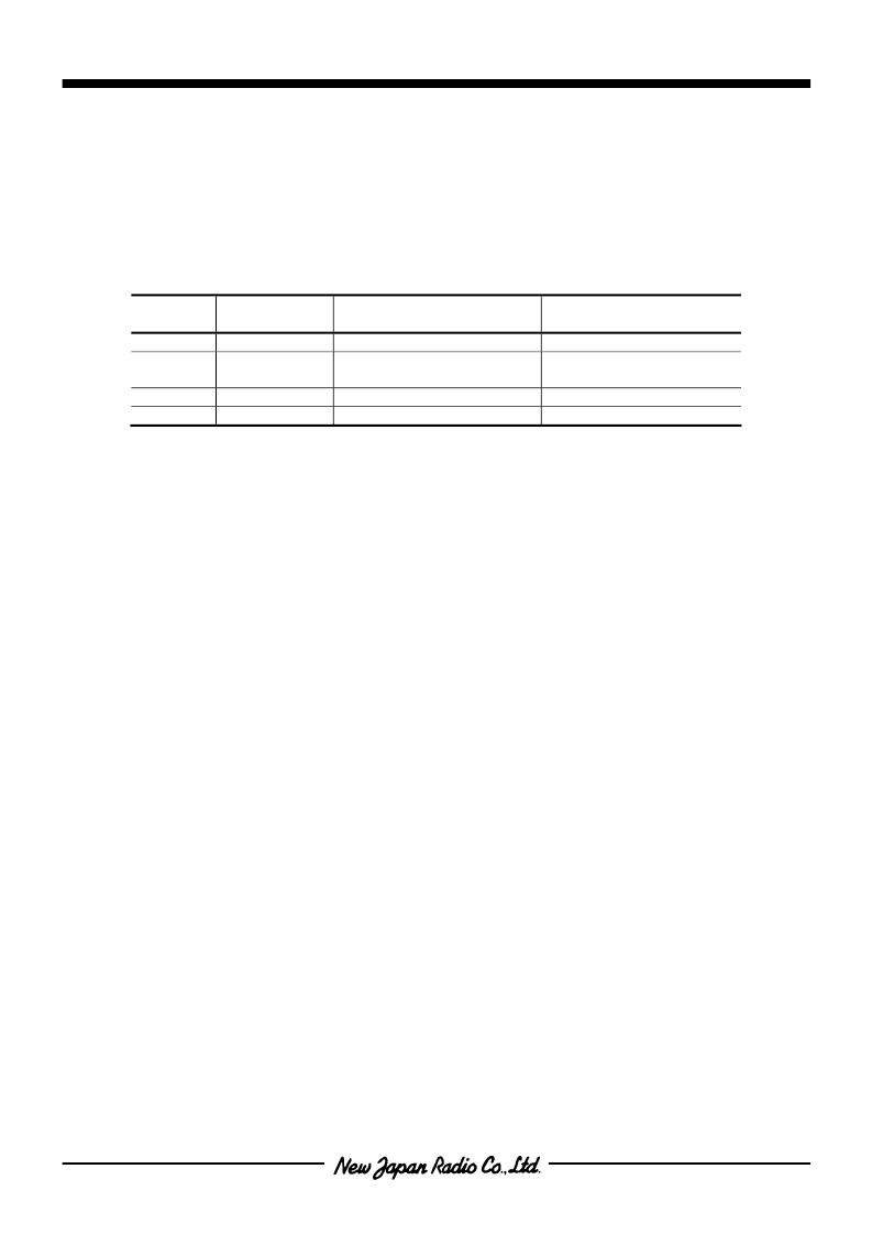
Table 5-1 Serial Host Interface Pin Description
Symbol
(I
2
C / Serial)
5
SCL/SCK
Serial Clock
Pin No.
4-Wire Serial bus Format
I
2
C bus Format
Serial Clock
Serial Data
(Bi-directional)
I
2
C bus address Bit1
I
2
C bus address Bit2
6
SDA/SDOUT
Serial Data Output
7
8
AD1/SDIN
AD2/SSb
Serial Data Input
SLAVE Select
Note : SDA /SDOUT pin is a bi-directional open drain.
SDA /SDOUT output is normal CMOS output in case of 4-Wire Serial bus mode and SSb=”Low”.
SDA /SDOUT output is Hi-Z state in case of 4-Wire Serial bus mode and SSb=”High”.
This pin requires a 4.7k pull-up resister in both 4-Wire serial and I
2
C bus mode.
5.1 4-Wire Serial Interface
The serial host interface can be configured for 4-Wire Serial bus communication by setting GPIO0 pin (*SEL1
pin)=”High” during the Reset initialization sequence. SHI bus communication is full-duplex; a write byte is shifted
into the SDIN pin at the same time that a read byte is shifted out of the SDOUT pin. Data transfers are MSB first
and are enabled by setting the Slave Select pin Low (SSb = 0). Data is clocked into SDIN on rising transitions of
SCK. Data is latched at SDOUT on falling transitions of SCK except for the first byte (MSB) which is latched on the
falling transitions of SSb. SDOUT is Hi-Z in case of SSb = “High”. SDOUT is CMOS output in case of SSb = “Low”.
SDOUT needs a pull-up resistor when SDOUT is Hi-Z.
*
It excepts NJU26150. Refer to each data sheet.
相關(guān)PDF資料 |
PDF描述 |
|---|---|
| NJW1165 | AUDIO PROCESSOR |
| NJW1165M | AUDIO PROCESSOR |
| NJW1165L | AUDIO PROCESSOR |
| NJW1167 | AUDIO PROCESSOR with Subwoofer Output |
| NJW1167V | AUDIO PROCESSOR with Subwoofer Output |
相關(guān)代理商/技術(shù)參數(shù) |
參數(shù)描述 |
|---|---|
| NJU26176 | 制造商:NJRC 制造商全稱:New Japan Radio 功能描述:NJU26100 Series Hardware Specification |
| NJU26177 | 制造商:NJRC 制造商全稱:New Japan Radio 功能描述:NJU26100 Series Hardware Specification |
| NJU26178 | 制造商:NJRC 制造商全稱:New Japan Radio 功能描述:NJU26100 Series Hardware Specification |
| NJU26179 | 制造商:NJRC 制造商全稱:New Japan Radio 功能描述:NJU26100 Series Hardware Specification |
| NJU26180 | 制造商:New Japan Radio Co Ltd (NJR/JRC) 功能描述: |
發(fā)布緊急采購(gòu),3分鐘左右您將得到回復(fù)。