- 您現(xiàn)在的位置:買賣IC網(wǎng) > PDF目錄382352 > MTV121 (Electronic Theatre Controls, Inc.) Super On-Screen-Display for LCD Monitor PDF資料下載
參數(shù)資料
| 型號: | MTV121 |
| 廠商: | Electronic Theatre Controls, Inc. |
| 英文描述: | Super On-Screen-Display for LCD Monitor |
| 中文描述: | 超級屏幕為液晶顯示器面板 |
| 文件頁數(shù): | 2/18頁 |
| 文件大?。?/td> | 220K |
| 代理商: | MTV121 |

2/18
MTV121 Revision 5.0 06/29/1999
MTV121
MYSON
TECHNOLOGY
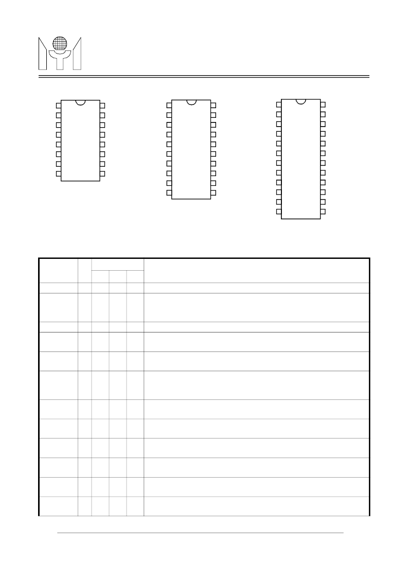
1.0 PIN CONNECTION
2.0 PIN DESCRIPTIONS
Name
I/O
Pin No.
Descriptions
N16 N20 N24
1
1
2
2
VSS
XIN
-
I
1
2
Ground.
This ground pin is used to internal circuitry.
Pixel clock input.
This is a clock input pin. MTV121 is driven by an exter-
nal pixel clock source for all the logics inside. The frequency of XIN must
be the integral time of pin HFLB.
No connection.
Power supply.
Positive 5 V DC supply for internal circuitry. And a 0.1uF
decoupling capacitor should be connected across to VDD and VSS.
Horizontal input.
This pin is used to input the horizontal synchronizing
signal. It is a leading edge triggered and has an internal pull-up resistor.
Serial interface enable.
It is used to enable the serial data and is also
used to select the operation of I
2
C or SPI bus. If this pin is left floating, I
2
C
bus is enabled, otherwise the SPI bus is enabled.
Serial data input.
The external data transfer through this pin to internal
display registers and control registers. It has an internal pull-up resistor.
Serial clock input.
The clock-input pin is used to synchronize the data
transfer. It has an internal pull-up resistor.
Open-Drain PWM D/A converter 0.
The output pulse width is program-
mable by the register of Row 15, Column 23.
Open-Drain PWM D/A converter 1.
The output pulse width is program-
mable by the register of Row 15, Column 24.
Open-Drain PWM D/A converter 2.
The output pulse width is program-
mable by the register of Row 15, Column 25.
Open-Drain PWM D/A converter 3.
The output pulse width is program-
mable by the register of Row 15, Column 26.
NC
VDD
I
-
3
4
3
4
3
4
HFLB
I
5
5
5
SSB
I
6
6
6
SDA
I
7
7
7
SCK
I
8
8
8
PWM0
O
-
9
9
PWM1
O
-
10
10
PWM2
O
-
-
11
PWM3
O
-
-
12
VSSA
XIN
NC
VDDA
HFLB
SSB
SDA
SCK
VSS
ROUT
GOUT
BOUT
FBKG
HTONE/PWMCK
VFLB
VDD
16
15
14
13
12
11
10
9
1
2
3
4
5
6
7
8
MTV121
VSSA
XIN
NC
VDDA
HFLB
SSB
SDA
SCK
PWM0
PWM1
PWM2
PWM3
VSS
ROUT
GOUT
BOUT
FBKG
HTONE/PWMCK
VFLB
VDD
PWM7
PWM6
PWM5
PWM4
24
23
22
21
20
19
18
17
16
15
14
13
1
2
3
4
5
6
7
8
9
10
11
12
MTV121N24
VSSA
XIN
NC
VDDA
HFLB
SSB
SDA
SCK
PWM0
PWM1
VSS
ROUT
GOUT
BOUT
FBKG
HTONE/PWMCK
VFLB
VDD
PWM7
PWM6
20
19
18
17
16
15
14
13
12
11
1
2
3
4
5
6
7
8
9
10
MTV121N20
相關(guān)PDF資料 |
PDF描述 |
|---|---|
| MUA08A | 265mW at 3.3V Supply Audio Power Amplifier with Shutdown Mode |
| MUB08A | 1W, Bypass-Capacitor-less Audio Amplifier with Internal Selectable Gain |
| MUBW10-06A7 | Converter - Brake - Inverter Module |
| MUBW10-06A6 | Converter - Brake - Inverter Module (CBI1) |
| MUBW10-12A6 | Converter - Brake - Inverter Module (CBI1) |
相關(guān)代理商/技術(shù)參數(shù) |
參數(shù)描述 |
|---|---|
| MTV1-21PL1 | 制造商:ITT Interconnect Solutions 功能描述:MTV1-21PL1 - Bulk |
| MTV1-21PS | 制造商:ITT Interconnect Solutions 功能描述:MTV1-21PS - Bulk |
| MTV1-21SAL1 | 制造商:ITT Interconnect Solutions 功能描述:MTV1-21SAL1 - Bulk |
| MTV1-21SH001 | 制造商:ITT Interconnect Solutions 功能描述:MTV1-21SH001 - Bulk |
| MTV1-21SL1 | 制造商:ITT Interconnect Solutions 功能描述:MTV1-21SL1 - Bulk |
發(fā)布緊急采購,3分鐘左右您將得到回復(fù)。