- 您現(xiàn)在的位置:買賣IC網(wǎng) > PDF目錄359234 > MT9072AV (ZARLINK SEMICONDUCTOR INC) Ultraframer DS3/E3/DS2/E2/DS1/E1/DS0 PDF資料下載
參數(shù)資料
| 型號: | MT9072AV |
| 廠商: | ZARLINK SEMICONDUCTOR INC |
| 元件分類: | 數(shù)字傳輸電路 |
| 英文描述: | Ultraframer DS3/E3/DS2/E2/DS1/E1/DS0 |
| 中文描述: | DATACOM, FRAMER, PBGA220 |
| 封裝: | 17 X 17 MM, 1.30 MM HEIGHT, MO-192, LBGA-220 |
| 文件頁數(shù): | 171/275頁 |
| 文件大?。?/td> | 3738K |
| 代理商: | MT9072AV |
第1頁第2頁第3頁第4頁第5頁第6頁第7頁第8頁第9頁第10頁第11頁第12頁第13頁第14頁第15頁第16頁第17頁第18頁第19頁第20頁第21頁第22頁第23頁第24頁第25頁第26頁第27頁第28頁第29頁第30頁第31頁第32頁第33頁第34頁第35頁第36頁第37頁第38頁第39頁第40頁第41頁第42頁第43頁第44頁第45頁第46頁第47頁第48頁第49頁第50頁第51頁第52頁第53頁第54頁第55頁第56頁第57頁第58頁第59頁第60頁第61頁第62頁第63頁第64頁第65頁第66頁第67頁第68頁第69頁第70頁第71頁第72頁第73頁第74頁第75頁第76頁第77頁第78頁第79頁第80頁第81頁第82頁第83頁第84頁第85頁第86頁第87頁第88頁第89頁第90頁第91頁第92頁第93頁第94頁第95頁第96頁第97頁第98頁第99頁第100頁第101頁第102頁第103頁第104頁第105頁第106頁第107頁第108頁第109頁第110頁第111頁第112頁第113頁第114頁第115頁第116頁第117頁第118頁第119頁第120頁第121頁第122頁第123頁第124頁第125頁第126頁第127頁第128頁第129頁第130頁第131頁第132頁第133頁第134頁第135頁第136頁第137頁第138頁第139頁第140頁第141頁第142頁第143頁第144頁第145頁第146頁第147頁第148頁第149頁第150頁第151頁第152頁第153頁第154頁第155頁第156頁第157頁第158頁第159頁第160頁第161頁第162頁第163頁第164頁第165頁第166頁第167頁第168頁第169頁第170頁當前第171頁第172頁第173頁第174頁第175頁第176頁第177頁第178頁第179頁第180頁第181頁第182頁第183頁第184頁第185頁第186頁第187頁第188頁第189頁第190頁第191頁第192頁第193頁第194頁第195頁第196頁第197頁第198頁第199頁第200頁第201頁第202頁第203頁第204頁第205頁第206頁第207頁第208頁第209頁第210頁第211頁第212頁第213頁第214頁第215頁第216頁第217頁第218頁第219頁第220頁第221頁第222頁第223頁第224頁第225頁第226頁第227頁第228頁第229頁第230頁第231頁第232頁第233頁第234頁第235頁第236頁第237頁第238頁第239頁第240頁第241頁第242頁第243頁第244頁第245頁第246頁第247頁第248頁第249頁第250頁第251頁第252頁第253頁第254頁第255頁第256頁第257頁第258頁第259頁第260頁第261頁第262頁第263頁第264頁第265頁第266頁第267頁第268頁第269頁第270頁第271頁第272頁第273頁第274頁第275頁
MT9072
Data Sheet
171
Zarlink Semiconductor Inc.
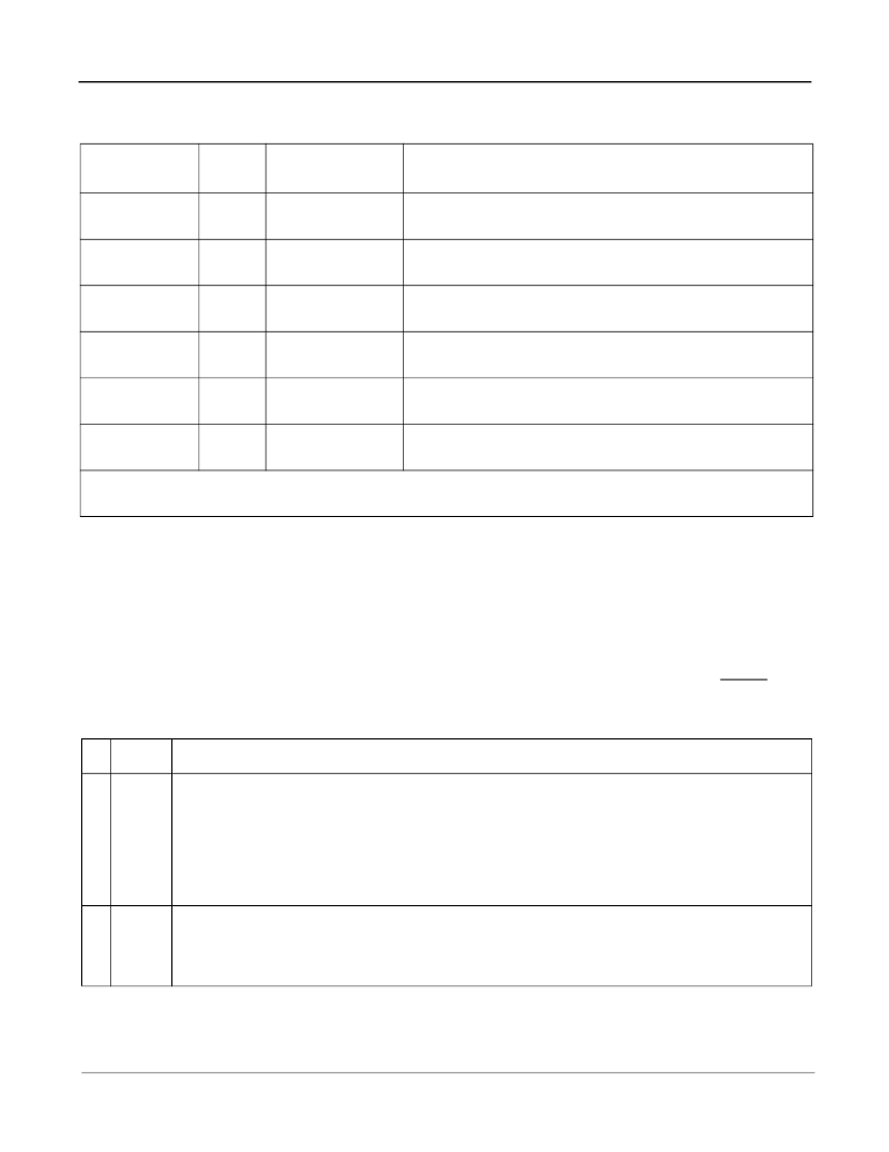
17.2.2.10 Receive National Bit Data Register(R/W) Address(YC0 to YC4) Summary
17.2.3 Master Control Registers (Y00 - Y09) Bit Functions
Tables 147 to 157 describe the bit functions of each of the Master Control Registers in the MT9072 in E1 Mode.
Each register is repeated for each of the 8 framers. Framer 0 is addressed with Y=0, Framer 1 with Y=1, Framer 2
with Y=2 and so on up to Framer 7 with Y=7 (where Y represents the 4 most significant address bits (MSB)
A11-A8). In addition, a simultaneous write to all 8 framers is possible by setting the MSB address to Y=8 (1000).
A (0), (1) or (#) in the “Name” column of these tables indicates the state of the data bits after a reset (RESET, RSTC
or RST). The (#) indicates that a (0) or (1) is possible.
Binary Address
(A
10
-A
0
)
Hex
Address
Register
Data Bits
(Upper byte B15 - B8 unused, B7 - B0 are shown)
yyyy 1111 1000
YC0
Receive National
Bits RN0 (Sa4)
RN0F1, RN0F3, RN0F5, RN0F7, RN0F9, RN0F11, RN0F13,
RN0F15
yyyy 1111 1001
YC1
Receive National
Bits RN1 (Sa5)
RN1F1, RN1F3, RN1F5, RN1F7, RN1F9, RN1F11, RN1F13,
RN1F15
yyyy 1111 1010
YC2
Receive National
Bits RN2 (Sa6)
RN2F1, RN2F3, RN2F5, RN2F7, RN2F9, RN2F11, RN2F13,
RN2F15
yyyy 1111 1011
YC3
Receive National
Bits RN3 (Sa7)
RN3F1, RN3F3, RN3F5, RN3F7, RN3F9, RN3F11, RN3F13,
RN3F15
yyyy 1111 0100
YC4
Receive National
Bits RN4 (Sa8)
RN4F1, RN4F3, RN4F5, RN4F7, RN4F9, RN4F11, RN4F13,
RN4F15
yyyy 1011 0101-
yyyy 1011 1111
YC5-YC
F
not used
not used
upper data byte (B15-8) is not used and may be any value if read
see the Register Group Address Summary for an explanation of yyyy and Y
Table 141 - Transmit National Bits Data Registers (R/W) Address (YFX) Summary (E1)
Bit
Name
Functional Description
15
IMA
Inverse Mux for ATM Mode.
Setting this bit high the I/O ports to allow for easy connection to one
of the Zarlink IMA devices such as the MT90220. DSTi becomes a serial 2.048 data stream. C4b
becomes a 4.096 MHz clock that clocks DSTi as the St-Bus. RXFPB becomes a framing pulse that
flags the E1 stream coming from the pin DSTo. The data from DSTo is clocked out on RXDLC. Set
this pin low for all other applications. Note that signalling operations CSTi/CSTo do not function
with the IMA Mode. The global control register 900 bit CK1 is ignored for this framer. 8.192 Mbit/s
backplane mode is not supported if IMA mode is selected on any one framer.
14
ASEL
(0)
AIS Select.
This bit selects the criteria on which the detection of a valid alarm indication signal
(AIS=1 of register address Y11) is based. If zero, the criteria is fewer than three zeros in a two
frame period (512 bits). If one, the criteria is fewer than three zeros in each of two consecutive
double-frame periods (512 bits per double-frame).
Table 142 - Alarm and Framing Control Register Y00 (R/W Address Y00) (E1)
相關(guān)PDF資料 |
PDF描述 |
|---|---|
| MT90820 | Large Digital Switch |
| MT90820AL | Large Digital Switch |
| MT90820AL1 | Large Digital Switch |
| MT90823AL1 | 3V Large Digital Switch |
| MT90823 | 3V Large Digital Switch |
相關(guān)代理商/技術(shù)參數(shù) |
參數(shù)描述 |
|---|---|
| MT9072AV2 | 制造商:Microsemi Corporation 功能描述:FRAMER E1/J1/T1 3.3V 220BGA - Trays 制造商:Zarlink Semiconductor Inc 功能描述:FRAMER E1/J1/T1 3.3V 220BGA - Trays |
| MT90732 | 制造商:MITEL 制造商全稱:Mitel Networks Corporation 功能描述:CMOS E2/E3 Framer (E2/E3F) |
| MT90732AP | 制造商:MITEL 制造商全稱:Mitel Networks Corporation 功能描述:CMOS E2/E3 Framer (E2/E3F) |
| MT90733 | 制造商:MITEL 制造商全稱:Mitel Networks Corporation 功能描述:CMOS DS3 Framer (DS3F) |
| MT90733AP | 制造商:MITEL 制造商全稱:Mitel Networks Corporation 功能描述:CMOS DS3 Framer (DS3F) |
發(fā)布緊急采購,3分鐘左右您將得到回復。