- 您現(xiàn)在的位置:買賣IC網(wǎng) > PDF目錄359234 > MT9072 (Zarlink Semiconductor Inc.) Ultraframer DS3/E3/DS2/E2/DS1/E1/DS0 PDF資料下載
參數(shù)資料
| 型號(hào): | MT9072 |
| 廠商: | Zarlink Semiconductor Inc. |
| 元件分類: | 通信及網(wǎng)絡(luò) |
| 英文描述: | Ultraframer DS3/E3/DS2/E2/DS1/E1/DS0 |
| 中文描述: | Ultraframer DS3/E3/DS2/E2/DS1/E1/DS0 |
| 文件頁數(shù): | 70/275頁 |
| 文件大小: | 3738K |
| 代理商: | MT9072 |
第1頁第2頁第3頁第4頁第5頁第6頁第7頁第8頁第9頁第10頁第11頁第12頁第13頁第14頁第15頁第16頁第17頁第18頁第19頁第20頁第21頁第22頁第23頁第24頁第25頁第26頁第27頁第28頁第29頁第30頁第31頁第32頁第33頁第34頁第35頁第36頁第37頁第38頁第39頁第40頁第41頁第42頁第43頁第44頁第45頁第46頁第47頁第48頁第49頁第50頁第51頁第52頁第53頁第54頁第55頁第56頁第57頁第58頁第59頁第60頁第61頁第62頁第63頁第64頁第65頁第66頁第67頁第68頁第69頁當(dāng)前第70頁第71頁第72頁第73頁第74頁第75頁第76頁第77頁第78頁第79頁第80頁第81頁第82頁第83頁第84頁第85頁第86頁第87頁第88頁第89頁第90頁第91頁第92頁第93頁第94頁第95頁第96頁第97頁第98頁第99頁第100頁第101頁第102頁第103頁第104頁第105頁第106頁第107頁第108頁第109頁第110頁第111頁第112頁第113頁第114頁第115頁第116頁第117頁第118頁第119頁第120頁第121頁第122頁第123頁第124頁第125頁第126頁第127頁第128頁第129頁第130頁第131頁第132頁第133頁第134頁第135頁第136頁第137頁第138頁第139頁第140頁第141頁第142頁第143頁第144頁第145頁第146頁第147頁第148頁第149頁第150頁第151頁第152頁第153頁第154頁第155頁第156頁第157頁第158頁第159頁第160頁第161頁第162頁第163頁第164頁第165頁第166頁第167頁第168頁第169頁第170頁第171頁第172頁第173頁第174頁第175頁第176頁第177頁第178頁第179頁第180頁第181頁第182頁第183頁第184頁第185頁第186頁第187頁第188頁第189頁第190頁第191頁第192頁第193頁第194頁第195頁第196頁第197頁第198頁第199頁第200頁第201頁第202頁第203頁第204頁第205頁第206頁第207頁第208頁第209頁第210頁第211頁第212頁第213頁第214頁第215頁第216頁第217頁第218頁第219頁第220頁第221頁第222頁第223頁第224頁第225頁第226頁第227頁第228頁第229頁第230頁第231頁第232頁第233頁第234頁第235頁第236頁第237頁第238頁第239頁第240頁第241頁第242頁第243頁第244頁第245頁第246頁第247頁第248頁第249頁第250頁第251頁第252頁第253頁第254頁第255頁第256頁第257頁第258頁第259頁第260頁第261頁第262頁第263頁第264頁第265頁第266頁第267頁第268頁第269頁第270頁第271頁第272頁第273頁第274頁第275頁
MT9072
Data Sheet
70
Zarlink Semiconductor Inc.
8.2.4 E1 Common Channel Signaling (CCS) Receive from PCM30 to CSTo and DSTo
The CSIG control bit (register address Y03) must be set to one for Common Channel signaling (CCS) operation.
CCS on the receive PCM30 link (bit positions one to eight of timeslots 15, 16 and/or 31 of every frame) is sourced
to the ST-BUS DSTo stream and may also be sourced to the ST-BUS CSTo stream. If the TS15E, TS16E & TS31E
control bits (register address Y06) are zero, the receive data will be sourced to the ST-BUS DSTo stream only,
timeslots 15, 16 and 31. If these bits are one, then the signaling data will be sourced to both the DSTo stream and
the ST-BUS CSTo stream. Note that any combination of the TS15E, TS16E & TS31E control bits (register address
Y06) may be enabled. The CSTo destination timeslots for the receive PCM30 timeslots 15, 16 and 31, are
determined respectively by the 15C4-15C0, 16C4-31C0 and 31C4-31C0 (register address Y07) programming bits.
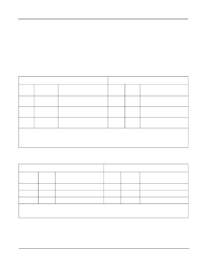
Table 29 shows the detailed bit mapping of CSTo timeslots from receive PCM30 frames. Table 30 shows the
detailed bit mapping of DSTo timeslots from receive PCM30 frames.
ST-BUS CSTo
PCM30 Receive
CRC-4
Frame
Timeslot
Data Bits (B7-B0)
Timeslot
CRC-4
Frame
Data Bits (B1-B8)
all
Any one of 32
n + m(0 to 31)
P1, P2, P3, P4, P5, P6, P7, P8
15
all
P1, P2, P3, P4, P5, P6, P7, P8
all
Any one of 32
n + m(0 to 31)
P1, P2, P3, P4, P5, P6, P7, P8
16
all
P1, P2, P3, P4, P5, P6, P7, P8
all
Any one of 32
n + m(0 to 31)
P1, P2, P3, P4, P5, P6, P7, P8
31
all
P1, P2, P3, P4, P5, P6, P7, P8
Note 1. For 2.048 Mbit/s operation, m=1 and n=0.
Note 2. For 8.192 Mbit/s operation, m=4 and n =0,1,2,3 where n corresponds to the framer number (i.e., n=0=framer 0... n=3= framer
3)
Note 3. For these functions to be valid, CCS mode must be selected (CSIG=1 register address Y03) and CSTo ST-BUS mode must
be selected (TS15E=1, TS16E=1 & TS31E=1 register address Y06) and the preferred destination CSTo timeslot should be selected
(15C4-0, 16C4-0 & 31C4-0 register address Y07).
Table 29 - Receive PCM30 CCS to ST-BUS 2.048 Mbit/s or 8.192 Mbit/s CSTo (E1)
ST-BUS DSTo
PCM30 Receive
CRC-4
Frame
Timeslot
Data Bits (B7-B0)
Timeslot
CRC-4
Frame
Data Bits (B1-B8)
all
n + m(15) P1, P2, P3, P4, P5, P6, P7, P8
15
all
P1, P2, P3, P4, P5, P6, P7, P8
all
n + m(16) P1, P2, P3, P4, P5, P6, P7, P8
16
all
P1, P2, P3, P4, P5, P6, P7, P8
all
n + m(31) P1, P2, P3, P4, P5, P6, P7, P8
31
all
P1, P2, P3, P4, P5, P6, P7, P8
Note 1. For 2.048 Mbit/s operation, m=1 and n=0.
Note 2. For 8.192 Mbit/s operation, m=4 and n =0,1,2,3 where n corresponds to the framer number (i.e., n=0=framer 0... n=3= framer
3)
Note 3. For these functions to be valid, CCS mode must be selected (CSIG=1 register address Y03).
Table 30 - Receive PCM30 CCS to ST-BUS 2.048 Mbit/s or 8.192 Mbit/s DSTo (E1)
相關(guān)PDF資料 |
PDF描述 |
|---|---|
| MT9072AB | Ultraframer DS3/E3/DS2/E2/DS1/E1/DS0 |
| MT9072AV | Ultraframer DS3/E3/DS2/E2/DS1/E1/DS0 |
| MT90820 | Large Digital Switch |
| MT90820AL | Large Digital Switch |
| MT90820AL1 | Large Digital Switch |
相關(guān)代理商/技術(shù)參數(shù) |
參數(shù)描述 |
|---|---|
| MT9072AB | 制造商:ZARLINK 制造商全稱:Zarlink Semiconductor Inc 功能描述:Octal T1/E1/J1 Framer |
| MT9072AV | 制造商:Microsemi Corporation 功能描述:FRAMER E1/J1/T1 3.3V 256BGA - Trays 制造商:Zarlink Semiconductor Inc 功能描述:FRAMER E1/J1/T1 3.3V 256BGA - Trays |
| MT9072AV2 | 制造商:Microsemi Corporation 功能描述:FRAMER E1/J1/T1 3.3V 220BGA - Trays 制造商:Zarlink Semiconductor Inc 功能描述:FRAMER E1/J1/T1 3.3V 220BGA - Trays |
| MT90732 | 制造商:MITEL 制造商全稱:Mitel Networks Corporation 功能描述:CMOS E2/E3 Framer (E2/E3F) |
| MT90732AP | 制造商:MITEL 制造商全稱:Mitel Networks Corporation 功能描述:CMOS E2/E3 Framer (E2/E3F) |
發(fā)布緊急采購,3分鐘左右您將得到回復(fù)。