- 您現(xiàn)在的位置:買賣IC網(wǎng) > PDF目錄384755 > MT46V64M8TG-8 (Micron Technology, Inc.) DOUBLE DATA RATE DDR SDRAM PDF資料下載
參數(shù)資料
| 型號(hào): | MT46V64M8TG-8 |
| 廠商: | Micron Technology, Inc. |
| 英文描述: | DOUBLE DATA RATE DDR SDRAM |
| 中文描述: | 雙倍數(shù)據(jù)速率的DDR SDRAM內(nèi)存 |
| 文件頁(yè)數(shù): | 56/68頁(yè) |
| 文件大?。?/td> | 2555K |
| 代理商: | MT46V64M8TG-8 |
第1頁(yè)第2頁(yè)第3頁(yè)第4頁(yè)第5頁(yè)第6頁(yè)第7頁(yè)第8頁(yè)第9頁(yè)第10頁(yè)第11頁(yè)第12頁(yè)第13頁(yè)第14頁(yè)第15頁(yè)第16頁(yè)第17頁(yè)第18頁(yè)第19頁(yè)第20頁(yè)第21頁(yè)第22頁(yè)第23頁(yè)第24頁(yè)第25頁(yè)第26頁(yè)第27頁(yè)第28頁(yè)第29頁(yè)第30頁(yè)第31頁(yè)第32頁(yè)第33頁(yè)第34頁(yè)第35頁(yè)第36頁(yè)第37頁(yè)第38頁(yè)第39頁(yè)第40頁(yè)第41頁(yè)第42頁(yè)第43頁(yè)第44頁(yè)第45頁(yè)第46頁(yè)第47頁(yè)第48頁(yè)第49頁(yè)第50頁(yè)第51頁(yè)第52頁(yè)第53頁(yè)第54頁(yè)第55頁(yè)當(dāng)前第56頁(yè)第57頁(yè)第58頁(yè)第59頁(yè)第60頁(yè)第61頁(yè)第62頁(yè)第63頁(yè)第64頁(yè)第65頁(yè)第66頁(yè)第67頁(yè)第68頁(yè)
56
512Mb: x4, x8, x16 DDR SDRAM
512Mx4x8x16DDR_B.p65
–
Rev. B; Pub 4/01
Micron Technology, Inc., reserves the right to change products or specifications without notice.
2001, Micron Technology, Inc.
512Mb: x4, x8, x16
DDR SDRAM
ADVANCE
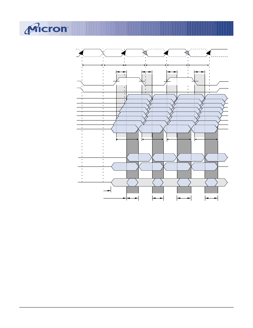
Figure 29
x4, x8 Data Output Timing
–
t
DQSQ,
t
QH and Data Valid Window
DQ (Last data valid)
DQ
2
DQ
2
DQ
2
DQ
2
DQ
2
DQ
2
DQS
1
DQ (Last data valid)
DQ (First data no longer valid)
DQ (First data no longer valid)
All DQs and DQS, collectively
6
NOTE:
1. DQs transitioning after DQS transition define tDQSQ window. DQS transitions at T2 and at T2n are an
“
early DQS,
”
at T3 is a
“
nominal DQS,
”
and at T3n is a "late DQS"
2. For a x4, only two DQs apply.
3. tDQSQ is derived at each DQS clock edge and is not cumulative over time and begins with DQS transition and
ends with the last valid transition of DQs .
4. tQH is derived from tHP : tQH = tHP - tQHS.
5. tHP is the lesser of tCL or tCH clock transition collectively when a bank is active.
6. The data valid window is derived for each DQS transitions and is defined as tQH minus tDQSQ.
Earliest signal transition
Latest signal transition
T2
T2
T2
T2n
T2n
T2n
T3
T3
T3
T3n
T3n
T3n
CK
CK#
T1
T2
T3
T4
T2n
T3n
tQH
4
tHP
5
tHP
5
tHP
5
tQH
4
tQH
4
tHP
5
tHP
5
tHP
5
tQH
4
tDQSQ
3
tDQSQ
3
tDQSQ
3
tDQSQ
3
Data
Valid
window
Data
Valid
window
Data
Valid
window
Data
Valid
window
QFC#
相關(guān)PDF資料 |
PDF描述 |
|---|---|
| MT46V64M8TG-8L | DOUBLE DATA RATE DDR SDRAM |
| MT48LC16M8A2 | SYNCHRONOUS DRAM |
| MT48LC2M32B2 | SYNCHRONOUS DRAM |
| MT48LC32M8A2 | SYNCHRONOUS DRAM |
| MT48LC16M16A2 | SYNCHRONOUS DRAM |
相關(guān)代理商/技術(shù)參數(shù) |
參數(shù)描述 |
|---|---|
| MT46V64M8TG-8L | 制造商:MICRON 制造商全稱:Micron Technology 功能描述:DOUBLE DATA RATE DDR SDRAM |
| MT46V8M16 | 制造商:MICRON 制造商全稱:Micron Technology 功能描述:DOUBLE DATA RATE DDR SDRAM |
發(fā)布緊急采購(gòu),3分鐘左右您將得到回復(fù)。