- 您現(xiàn)在的位置:買賣IC網(wǎng) > PDF目錄359218 > MRF6S27085HR3 (飛思卡爾半導(dǎo)體(中國)有限公司) N-Channel Enhancement-Mode Lateral MOSFETs PDF資料下載
參數(shù)資料
| 型號: | MRF6S27085HR3 |
| 廠商: | 飛思卡爾半導(dǎo)體(中國)有限公司 |
| 英文描述: | N-Channel Enhancement-Mode Lateral MOSFETs |
| 中文描述: | N溝道增強型MOSFET的外側(cè) |
| 文件頁數(shù): | 1/12頁 |
| 文件大小: | 358K |
| 代理商: | MRF6S27085HR3 |
MRF6S27085HR3 MRF6S27085HSR3
1
RF Device Data
Freescale Semiconductor
RF Power Field Effect Transistors
N-Channel Enhancement-Mode Lateral MOSFETs
Designed for N-CDMA base station applications with frequencies from 2600
to 2700 MHz. Suitable for TDMA, CDMA and multicarrier amplifier applica-
tions. To be used in Class AB for PCN - PCS/cellular radio and WLL
applications.
Typical Single-Carrier N-CDMA Performance: V
DD
= 28 Volts, I
DQ
=
900 mA, P
out
= 20 Watts Avg., Full Frequency Band, IS-95 CDMA (Pilot,
Sync, Paging, Traffic Codes 8 Through 13) Channel Bandwidth =
1.2288 MHz. Peak/Avg. = 9.8 dB @ 0.01% Probability on CCDF.
Power Gain — 15.5 dB
Drain Efficiency — 23.5%
ACPR @ 885 kHz Offset — -48 dBc @ 30 kHz Bandwidth
Capable of Handling 10:1 VSWR, @ 28 Vdc, 2700 MHz, 85 Watts CW
Output Power
Characterized with Series Equivalent Large-Signal Impedance Parameters
Internally Matched, Controlled Q, for Ease of Use
Qualified Up to a Maximum of 32 V
DD
Operation
Integrated ESD Protection
Lower Thermal Resistance Package
Designed for Lower Memory Effects and Wide Instantaneous Bandwidth
Applications
Low Gold Plating Thickness on Leads, 40
μ″
Nominal.
In Tape and Reel. R3 Suffix = 250 Units per 56 mm, 13 inch Reel.
Table 1. Maximum Ratings
Rating
Symbol
Value
Unit
Drain-Source Voltage
V
DSS
-0.5, +68
Vdc
Gate-Source Voltage
V
GS
-0.5, +12
Vdc
Total Device Dissipation @ T
C
= 25
°
C
Derate above 25
°
C
P
D
350
2
W
W/
°
C
Storage Temperature Range
T
stg
- 65 to +150
°
C
Operating Junction Temperature
T
J
200
°
C
CW Operation
CW
85
W
Table 2. Thermal Characteristics
Characteristic
Symbol
Value
(1,2)
Unit
Thermal Resistance, Junction to Case
Case Temperature 80
°
C, 85 W CW
Case Temperature 76
°
C, 20 W CW
R
θ
JC
0.50
0.56
°
C/W
1. MTTF calculator available at http://www.freescale.com/rf. Select Tools/Software/Application Software/Calculators to access
the MTTF calculators by product.
2. Refer to AN1955/D,
Thermal Measurement Methodology of RF Power Amplifiers.
Go to http://www.freescale.com/rf.
Select Documentation/Application Notes - AN1955.
NOTE -
CAUTION
- MOS devices are susceptible to damage from electrostatic charge. Reasonable precautions in handling and
packaging MOS devices should be observed.
Document Number: MRF6S27085H
Rev. 1, 1/2005
Freescale Semiconductor
Technical Data
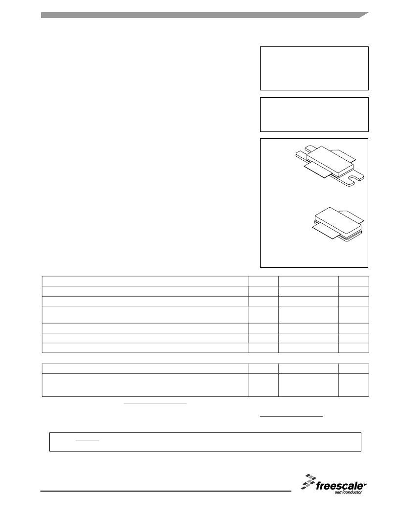
MRF6S27085HR3
MRF6S27085HSR3
2700 MHz, 20 W AVG., 28 V
SINGLE N-CDMA
LATERAL N-CHANNEL
RF POWER MOSFETs
CASE 465A-06, STYLE 1
NI-780S
MRF6S27085HSR3
CASE 465-06, STYLE 1
NI-780
MRF6S27085HR3
Freescale Semiconductor, Inc., 2005. All rights reserved.
相關(guān)PDF資料 |
PDF描述 |
|---|---|
| MRF6S9045N | RF Power Field Effect Transistors |
| MRF6S9045 | RF Power Field Effect Transistors |
| MRF6S9045MBR1 | RF Power Field Effect Transistors |
| MRF6S9045MR1 | RF Power Field Effect Transistors |
| MRF6S9045NR1 | RF Power Field Effect Transistors |
相關(guān)代理商/技術(shù)參數(shù) |
參數(shù)描述 |
|---|---|
| MRF6S27085HR3_06 | 制造商:FREESCALE 制造商全稱:Freescale Semiconductor, Inc 功能描述:RF Power Field Effect Transistors |
| MRF6S27085HR3_08 | 制造商:FREESCALE 制造商全稱:Freescale Semiconductor, Inc 功能描述:RF Power Field Effect Transistors N-Channel Enhancement-Mode Lateral MOSFETs |
| MRF6S27085HR5 | 功能描述:射頻MOSFET電源晶體管 HV6 2700MHZ NCDMA NI780H RoHS:否 制造商:Freescale Semiconductor 配置:Single 晶體管極性: 頻率:1800 MHz to 2000 MHz 增益:27 dB 輸出功率:100 W 汲極/源極擊穿電壓: 漏極連續(xù)電流: 閘/源擊穿電壓: 最大工作溫度: 封裝 / 箱體:NI-780-4 封裝:Tray |
| MRF6S27085HS | 制造商:Freescale Semiconductor 功能描述: |
| MRF6S27085HSR3 | 功能描述:射頻MOSFET電源晶體管 HV6 2700MHZ NCDMA NI780H RoHS:否 制造商:Freescale Semiconductor 配置:Single 晶體管極性: 頻率:1800 MHz to 2000 MHz 增益:27 dB 輸出功率:100 W 汲極/源極擊穿電壓: 漏極連續(xù)電流: 閘/源擊穿電壓: 最大工作溫度: 封裝 / 箱體:NI-780-4 封裝:Tray |
發(fā)布緊急采購,3分鐘左右您將得到回復(fù)。