- 您現(xiàn)在的位置:買賣IC網(wǎng) > PDF目錄18711 > MPC8377EWLANB (Freescale Semiconductor)ACCESS POINT/ROUTER MPC8377 PDF資料下載
參數(shù)資料
| 型號: | MPC8377EWLANB |
| 廠商: | Freescale Semiconductor |
| 文件頁數(shù): | 106/127頁 |
| 文件大小: | 0K |
| 描述: | ACCESS POINT/ROUTER MPC8377 |
| 標準包裝: | 1 |
第1頁第2頁第3頁第4頁第5頁第6頁第7頁第8頁第9頁第10頁第11頁第12頁第13頁第14頁第15頁第16頁第17頁第18頁第19頁第20頁第21頁第22頁第23頁第24頁第25頁第26頁第27頁第28頁第29頁第30頁第31頁第32頁第33頁第34頁第35頁第36頁第37頁第38頁第39頁第40頁第41頁第42頁第43頁第44頁第45頁第46頁第47頁第48頁第49頁第50頁第51頁第52頁第53頁第54頁第55頁第56頁第57頁第58頁第59頁第60頁第61頁第62頁第63頁第64頁第65頁第66頁第67頁第68頁第69頁第70頁第71頁第72頁第73頁第74頁第75頁第76頁第77頁第78頁第79頁第80頁第81頁第82頁第83頁第84頁第85頁第86頁第87頁第88頁第89頁第90頁第91頁第92頁第93頁第94頁第95頁第96頁第97頁第98頁第99頁第100頁第101頁第102頁第103頁第104頁第105頁當前第106頁第107頁第108頁第109頁第110頁第111頁第112頁第113頁第114頁第115頁第116頁第117頁第118頁第119頁第120頁第121頁第122頁第123頁第124頁第125頁第126頁第127頁
MPC8377E PowerQUICC II Pro Processor Hardware Specifications, Rev. 8
8
Freescale Semiconductor
2.1.2
Power Supply Voltage Specification
This table provides recommended operating conditions for the device. Note that the values in this table are
the recommended and tested operating conditions. Proper device operation outside of these conditions is
not guaranteed.
Input voltage
DDR DRAM signals
MVIN
–0.3 to (GVDD + 0.3)
V
DDR DRAM reference
MVREF
–0.3 to (GVDD + 0.3)
V
Three-speed Ethernet signals
LVIN
–0.3 to (LVDD + 0.3)
V
—
PCI, DUART, CLKIN, system control and power
management, I2C, and JTAG signals
OVIN
–0.3 to (OVDD + 0.3)
V
Local Bus
LBIN
–0.3 to (LBVDD + 0.3)
V
—
Storage temperature range
TSTG
–55 to 150
°C—
Notes:
1. Functional and tested operating conditions are given in Table 3. Absolute maximum ratings are stress ratings only, and
functional operation at the maximums is not guaranteed. Stresses beyond those listed may affect device reliability or cause
permanent damage to the device.
2. Caution: MVIN must not exceed GVDD by more than 0.3 V. This limit may be exceeded for a maximum of 20 ms during
power-on reset and power-down sequences.
3. Caution: OVIN must not exceed OVDD by more than 0.3 V. This limit may be exceeded for a maximum of 20 ms during
power-on reset and power-down sequences.
4. (M,O)VIN and MVREF may overshoot/undershoot to a voltage and for a maximum duration as shown in Figure 2.
5. Overshoot/undershoot by OVIN on the PCI interface does not comply to the PCI Electrical Specification for 3.3-V operation,
as shown in Figure 2.
6. L[1,2]_
nVDD includes SDAVDD_0, XCOREVDD, and XPADVDD power inputs.
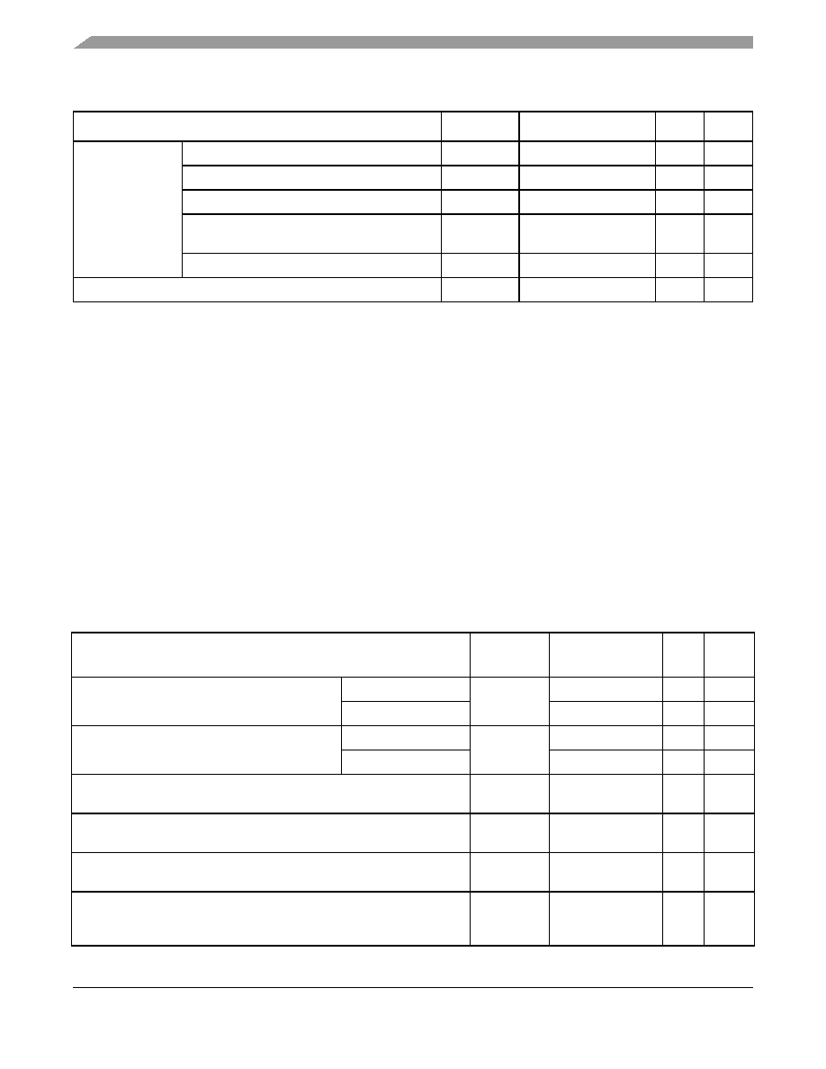
Table 3. Recommended Operating Conditions
Characteristic
Symbol
Recommended
Value
Unit
Note
Core supply voltage
up to 667 MHz
VDD
1.0 ± 50 mV
V
800 MHz
1.05 ± 50 mV
V
PLL supply voltage (e300 core, eLBC and
system)
up to 667 MHz
AVDD
1.0 ± 50 mV
V
800 MHz
1.05 ± 50 mV
V
DDR1 and DDR2 DRAM I/O voltage
GVDD
2.5 V ± 125 mV
1.8 V ± 90 mV
Three-speed Ethernet I/O, MII management voltage
LVDD[1,2]
3.3 V ± 165 mV
2.5 V ± 125 mV
V—
PCI, local bus, DUART, system control and power management, I2C, and
JTAG I/O voltage
OVDD
3.3 V ± 165 mV
V
Local Bus
LBVDD
1.8 V ± 90 mV
2.5 V ± 125 mV
3.3 V ± 165 mV
V—
Table 2. Absolute Maximum Ratings1 (continued)
Characteristic
Symbol
Max Value
Unit
Note
相關(guān)PDF資料 |
PDF描述 |
|---|---|
| 0622022010 | TOOL INSERTION 40POS 4ROWS |
| MPC8377EWLANA | ACCESS POINT/ROUTER MPC8377 |
| 76250ENC | XFRMR MAX250 EN60950 APPROVED |
| DR-TRC105-434-EV | BOARD EVALUATION 434MHZ RFM RFIC |
| DR-TRC105-403-EV | BOARD EVALUATION 403MHZ RFM RFIC |
相關(guān)代理商/技術(shù)參數(shù) |
參數(shù)描述 |
|---|---|
| MPC8377EZQAFDA | 制造商:FREESCALE 制造商全稱:Freescale Semiconductor, Inc 功能描述:PowerQUICC? II Pro Processor Hardware Specifications |
| MPC8377EZQAFFA | 制造商:FREESCALE 制造商全稱:Freescale Semiconductor, Inc 功能描述:PowerQUICC? II Pro Processor Hardware Specifications |
| MPC8377EZQAFGA | 制造商:FREESCALE 制造商全稱:Freescale Semiconductor, Inc 功能描述:PowerQUICC? II Pro Processor Hardware Specifications |
| MPC8377EZQAGDA | 制造商:FREESCALE 制造商全稱:Freescale Semiconductor, Inc 功能描述:PowerQUICC? II Pro Processor Hardware Specifications |
| MPC8377EZQAGFA | 制造商:FREESCALE 制造商全稱:Freescale Semiconductor, Inc 功能描述:PowerQUICC? II Pro Processor Hardware Specifications |
發(fā)布緊急采購,3分鐘左右您將得到回復(fù)。