- 您現(xiàn)在的位置:買賣IC網(wǎng) > PDF目錄371088 > MCM63R736 (Motorola, Inc.) 4MBit Synchronous Late Write Fast Static RAM(4M位同步遲寫快速靜態(tài)RAM) PDF資料下載
參數(shù)資料
| 型號: | MCM63R736 |
| 廠商: | Motorola, Inc. |
| 英文描述: | 4MBit Synchronous Late Write Fast Static RAM(4M位同步遲寫快速靜態(tài)RAM) |
| 中文描述: | 晚寫的4Mb同步快速靜態(tài)存儲器(4分位同步遲寫快速靜態(tài)內(nèi)存) |
| 文件頁數(shù): | 6/21頁 |
| 文件大?。?/td> | 311K |
| 代理商: | MCM63R736 |
MCM63R736
MCM63R818
6
MOTOROLA FAST SRAM
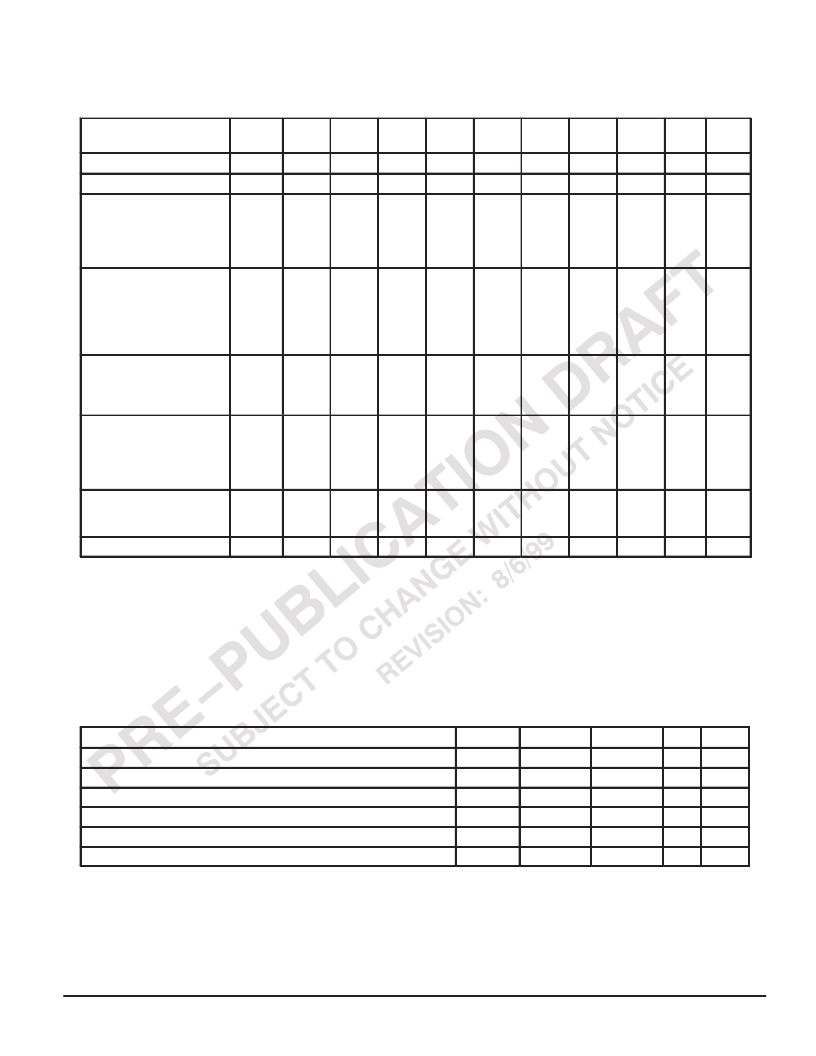
DC OPERATING CONDITIONS AND CHARACTERISTICS
(2.375 V
≤
VDD
≤
3.6 V, 0
°
C
≤
TA
≤
70
°
C, Unless Otherwise Noted)
RECOMMENDED OPERATING CONDITIONS
(See Notes 1 through 4)
Parameter
Symbol
Min
Typical
–3
Typical
–3.3
Typical
–3.7
Typical
–4
Typical
–4.4
Typical
–5
Max
Unit
Notes
Core Power Supply Voltage
VDD
VDDQ
IDD1
2.375
—
—
—
3.6
V
Output Driver Supply Voltage
1.4
—
—
—
2.0
V
AC Supply Current (Device
Selected, All Outputs Open,
Freq = Max, VDD = Max,
VDDQ = Max). Includes
Supply Currents for VDD.
—
400
380
360
340
320
300
—
mA
5
Quiescent Active Power
Supply Current (Device
Selected, All Outputs Open,
Freq = 0, VDD = Max,
VDDQ = Max). Includes
Supply Currents for VDD.
IDD2
—
175
175
175
175
175
175
—
mA
6
Active Standby Power
Supply Current (Device
Deselected, Freq = Max,
VDD = Max, VDDQ = Max).
CMOS Standby Supply
Current (Device Deselected,
Freq = 0, VDD = Max,
VDDQ = Max, All Inputs
Static at CMOS Levels).
ISB1
—
200
195
190
185
180
175
—
mA
7
ISB2
—
175
175
175
175
175
175
—
mA
6, 7
Sleep Mode Current
(ZZ = VIH, VDD = Max,
VDDQ = Max)
IZZ
—
50
50
50
50
50
50
—
mA
6, 7
Input Reference DC Voltage
Vref (dc)
0.6
—
—
—
—
—
—
1.3
V
8
NOTES:
1. All data sheet parameters specified to full range of VDD unless otherwise noted. All voltages are referenced to voltage applied to VSS bumps.
2. Supply voltage applied to VDD connections.
3. Supply voltage applied to VDDQ connections.
4. All power supply currents measured with outputs open or deselected.
5. All inputs are zero.
6. CMOS levels for I/Os are VIC
≤
VSS + 0.2 V or
≥
VDDQ – 0.2 V.
7. Device deselected as defined by the Clock Truth Table.
8. Although considerable latitude in the selection of the nominal dc value (i.e., rms value) of Vref is supported, the peak–to–peak ac component
superimposed on Vref may not exceed 5% of the dc component of Vref.
DC INPUT CHARACTERISTICS
Parameter
Symbol
Min
Max
Unit
Notes
DC Input Logic High
VIH (dc)
VIL (dc)
Ilkg(I)
Vin (dc)
VDIF (dc)
VCM (dc)
Vref + 0.1
–0.3
VDDQ + 0.3
Vref – 0.1
±
5
V
DC Input Logic Low
V
1
Input Leakage Current
—
μ
A
2
Clock Input Signal Voltage
–0.3
2.5
V
Clock Input Differential Voltage (See Figure 3)
0.2
2.5
V
3
Clock Input Common Mode Voltage Range (See Figure 3)
NOTES:
1. Inputs may undershoot to –1.5 V (peak) for up to 35% tKHKH (e.g., 1.5 ns at a clock cycle time of 4.4 ns). See FIgure 2.
2. 0 V
≤
Vin
≤
VDDQ for all pins.
3. Minimum instantaneous differential input voltage required for differential input clock operation.
4. Maximum rejectable common mode input voltage variation.
0.60
1.1
V
4
相關(guān)PDF資料 |
PDF描述 |
|---|---|
| MCM63R819 | 4MBit Synchronous Late Write Fast Static RAM(4M位同步遲寫快速靜態(tài)RAM) |
| MCM63R836 | 8MBit Synchronous Late Write Fast Static RAM(8M位同步遲寫快速靜態(tài)RAM) |
| MCM63R918 | 8MBit Synchronous Late Write Fast Static RAM(8M位同步遲寫快速靜態(tài)RAM) |
| MCM63R918A | 8MBit Synchronous Late Write Fast Static RAM(8M位同步遲寫快速靜態(tài)RAM) |
| MCM63R836A | 8MBit Synchronous Late Write Fast Static RAM(8M位同步遲寫快速靜態(tài)RAM) |
相關(guān)代理商/技術(shù)參數(shù) |
參數(shù)描述 |
|---|---|
| MCM63R836 | 制造商:FREESCALE 制造商全稱:Freescale Semiconductor, Inc 功能描述:MCM63R836 |
| MCM63R836A | 制造商:FREESCALE 制造商全稱:Freescale Semiconductor, Inc 功能描述:8M Late Write HSTL |
| MCM63R836FC3.0 | 制造商:FREESCALE 制造商全稱:Freescale Semiconductor, Inc 功能描述:MCM63R836 |
| MCM63R836FC3.0R | 制造商:FREESCALE 制造商全稱:Freescale Semiconductor, Inc 功能描述:MCM63R836 |
| MCM63R836FC3.3 | 制造商:FREESCALE 制造商全稱:Freescale Semiconductor, Inc 功能描述:MCM63R836 |
發(fā)布緊急采購,3分鐘左右您將得到回復(fù)。