- 您現(xiàn)在的位置:買賣IC網(wǎng) > PDF目錄45312 > MCF5372LCVM240 (FREESCALE SEMICONDUCTOR INC) 32-BIT, 240 MHz, RISC PROCESSOR, PBGA196 PDF資料下載
參數(shù)資料
| 型號(hào): | MCF5372LCVM240 |
| 廠商: | FREESCALE SEMICONDUCTOR INC |
| 元件分類: | 微控制器/微處理器 |
| 英文描述: | 32-BIT, 240 MHz, RISC PROCESSOR, PBGA196 |
| 封裝: | 15 X 15 MM, ROHS COMPLIANT, MAPBGA-196 |
| 文件頁數(shù): | 10/46頁 |
| 文件大?。?/td> | 922K |
| 代理商: | MCF5372LCVM240 |
第1頁第2頁第3頁第4頁第5頁第6頁第7頁第8頁第9頁當(dāng)前第10頁第11頁第12頁第13頁第14頁第15頁第16頁第17頁第18頁第19頁第20頁第21頁第22頁第23頁第24頁第25頁第26頁第27頁第28頁第29頁第30頁第31頁第32頁第33頁第34頁第35頁第36頁第37頁第38頁第39頁第40頁第41頁第42頁第43頁第44頁第45頁第46頁
MCF537x ColdFire Microprocessor Data Sheet, Rev. 4
Electrical Characteristics
Freescale Semiconductor
18
5.6
External Interface Timing Characteristics
Table 9 lists processor bus input timings.
NOTE
All processor bus timings are synchronous; that is, input setup/hold and output delay with
respect to the rising edge of a reference clock. The reference clock is the FB_CLK output.
All other timing relationships can be derived from these values. Timings listed in Table 9
14
Discrete load capacitance for EXTAL
CL_EXTAL
2*CL–-
CS_EXTAL –
CPCB_EXTAL
pF
17
Peak-to-peak Jitter (Clock edge to clock edge)
Long Term Jitter
Cjitter
—
10
TBD
% fsys/3
18
Frequency Modulation Range Limit 3, 10, 11
(fsysMax must not be exceeded)
Cmod
0.8
2.2
%fsys/3
19
VCO Frequency. fvco = (fref * PFD)/4
fvco
350
540
MHz
1 The maximum allowable input clock frequency when booting with the PLL enabled is 24MHz. For higher input clock
frequencies the processor must boot in LIMP mode to avoid violating the maximum allowable CPU frequency.
2 All internal registers retain data at 0 Hz.
3 This parameter is guaranteed by characterization before qualification rather than 100% tested.
4 Proper PC board layout procedures must be followed to achieve specifications.
5 This parameter is guaranteed by design rather than 100% tested.
6 This specification is the PLL lock time only and does not include oscillator start-up time.
7 C
PCB_EXTAL and CPCB_XTAL are the measured PCB stray capacitances on EXTAL and XTAL, respectively.
8 Jitter is the average deviation from the programmed frequency measured over the specified interval at maximum f
sys.
Measurements are made with the device powered by filtered supplies and clocked by a stable external clock signal.
Noise injected into the PLL circuitry via PLL VDD, EVDD, and VSS and variation in crystal oscillator frequency increase
the Cjitter percentage for a given interval.
9 Values are with frequency modulation disabled. If frequency modulation is enabled, jitter is the sum of Cjitter+Cmod.
10 Modulation percentage applies over an interval of 10
μs, or equivalently the modulation rate is 100 KHz.
11 Modulation range determined by hardware design.
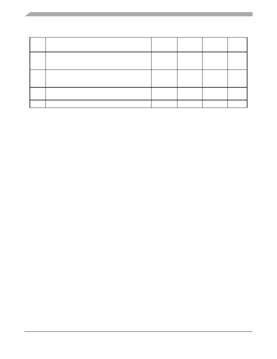
Table 8. PLL Electrical Characteristics (continued)
Num
Characteristic
Symbol
Min.
Value
Max.
Value
Unit
Because
of
an
order
from
the
United
States
International
Trade
Commission,
BGA-packaged
product
lines
and
part
numbers
indicated
here
currently
are
not
available
from
Freescale
for
import
or
sale
in
the
United
States
prior
to
September
2010:
MCF53721CVM240,
MCF5372LCVM240,
MCF5373LCVM240
相關(guān)PDF資料 |
PDF描述 |
|---|---|
| MCF5407FT162 | 32-BIT, 162 MHz, RISC PROCESSOR, PQFP208 |
| MCF5407FT220 | 32-BIT, 220 MHz, RISC PROCESSOR, PQFP208 |
| MCF5407CFT162 | 32-BIT, 162 MHz, RISC PROCESSOR, PQFP208 |
| MCF54450VM180 | 32-BIT, 180 MHz, RISC PROCESSOR, BGA256 |
| MCF54454VR266 | 32-BIT, 266 MHz, RISC PROCESSOR, PBGA360 |
相關(guān)代理商/技術(shù)參數(shù) |
參數(shù)描述 |
|---|---|
| MCF5372LCVM240J | 功能描述:32位微控制器 - MCU V3CORE RoHS:否 制造商:Texas Instruments 核心:C28x 處理器系列:TMS320F28x 數(shù)據(jù)總線寬度:32 bit 最大時(shí)鐘頻率:90 MHz 程序存儲(chǔ)器大小:64 KB 數(shù)據(jù) RAM 大小:26 KB 片上 ADC:Yes 工作電源電壓:2.97 V to 3.63 V 工作溫度范圍:- 40 C to + 105 C 封裝 / 箱體:LQFP-80 安裝風(fēng)格:SMD/SMT |
| MCF5373 | 制造商:FREESCALE 制造商全稱:Freescale Semiconductor, Inc 功能描述:ColdFire㈢ Microprocessor |
| MCF5373_08 | 制造商:FREESCALE 制造商全稱:Freescale Semiconductor, Inc 功能描述:ColdFire㈢ Microprocessor |
| MCF5373CAB180 | 制造商:FREESCALE 制造商全稱:Freescale Semiconductor, Inc 功能描述:Microprocessor Data Sheet |
| MCF5373L | 制造商:FREESCALE 制造商全稱:Freescale Semiconductor, Inc 功能描述:ColdFire㈢ Microprocessor |
發(fā)布緊急采購,3分鐘左右您將得到回復(fù)。