- 您現(xiàn)在的位置:買賣IC網(wǎng) > PDF目錄359730 > MC9328MX21CVM (Motorola, Inc.) i.MX family of microprocessors PDF資料下載
參數(shù)資料
| 型號: | MC9328MX21CVM |
| 廠商: | Motorola, Inc. |
| 英文描述: | i.MX family of microprocessors |
| 中文描述: | i.MX系列微處理器 |
| 文件頁數(shù): | 88/96頁 |
| 文件大?。?/td> | 1495K |
| 代理商: | MC9328MX21CVM |
第1頁第2頁第3頁第4頁第5頁第6頁第7頁第8頁第9頁第10頁第11頁第12頁第13頁第14頁第15頁第16頁第17頁第18頁第19頁第20頁第21頁第22頁第23頁第24頁第25頁第26頁第27頁第28頁第29頁第30頁第31頁第32頁第33頁第34頁第35頁第36頁第37頁第38頁第39頁第40頁第41頁第42頁第43頁第44頁第45頁第46頁第47頁第48頁第49頁第50頁第51頁第52頁第53頁第54頁第55頁第56頁第57頁第58頁第59頁第60頁第61頁第62頁第63頁第64頁第65頁第66頁第67頁第68頁第69頁第70頁第71頁第72頁第73頁第74頁第75頁第76頁第77頁第78頁第79頁第80頁第81頁第82頁第83頁第84頁第85頁第86頁第87頁當前第88頁第89頁第90頁第91頁第92頁第93頁第94頁第95頁第96頁
MC9328MX1 Advance Information, Rev. 4
88
Freescale Semiconductor
Specifications
3.22 CMOS Sensor Interface
The CSI module consists of a control register to configure the interface timing, a control register for statistic data
generation, a status register, interface logic, a 32
×
32 image data receive FIFO, and a 16
×
32 statistic data FIFO.
3.22.1 Gated Clock Mode
Figure 68 shows the timing diagram when the CMOS sensor output data is configured for negative edge and the
CSI is programmed to received data on the positive edge. Figure 69 on page 89 shows the timing diagram when the
CMOS sensor output data is configured for positive edge and the CSI is programmed to received data in negative
edge. The parameters for the timing diagrams are listed in Table 42 on page 89.
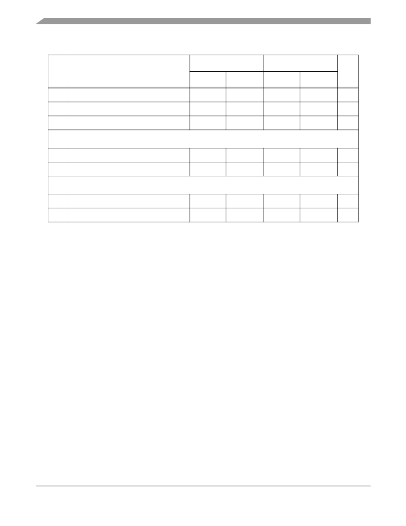
28
STCK high to STXD high impedance
17.90
29.75
15.7
26.1
ns
29
SRXD setup time before SRCK low
1.14
–
1.0
–
ns
30
SRXD hole time after SRCK low
0
–
0
–
ns
Synchronous Internal Clock Operation (Port B Alternate Function)
2
31
SRXD setup before STCK falling
18.81
–
16.5
–
ns
32
SRXD hold after STCK falling
0
–
0
–
ns
Synchronous External Clock Operation (Port B Alternate Function)
2
33
SRXD setup before STCK falling
1.14
–
1.0
–
ns
34
SRXD hold after STCK falling
0
–
0
–
ns
1.
All the timings for both SSI modules are given for a non-inverted serial clock polarity (TSCKP/RSCKP =
0) and a non-inverted frame sync (TFSI/RFSI = 0). If the polarity of the clock and/or the frame sync have
been inverted, all the timing remains valid by inverting the clock signal STCK/SRCK and/or the frame sync
STFS/SRFS shown in the tables and in the figures.
There is one set of I/O signals for the SSI2 module. They are from Port C alternate function (PC19 –
PC24). When SSI signals are configured as outputs, they can be viewed at Port C alternate function a.
When SSI signals are configured as inputs, the SSI module selects the input based on FMCR register bits
in the Clock controller module (CRM). By default, the input is selected from Port C alternate function.
bl = bit length; wl = word length
2.
3.
Table 41. SSI 2 Timing Parameter Table (Continued)
Ref
No.
Parameter
1.8V +/- 0.10V
3.0V +/- 0.30V
Unit
Minimum
Maximum
Minimum
Maximum
相關PDF資料 |
PDF描述 |
|---|---|
| MC68HC711E9CFN2 | Microcontrollers |
| MC68HC711E9CFN3 | Microcontrollers |
| MC68HC711E9CFS2 | Microcontrollers |
| MC68HC711E9CFS3 | Microcontrollers |
| MC68HC11A0CFN3 | HCMOS Single-Chip Microcontroller |
相關代理商/技術參數(shù) |
參數(shù)描述 |
|---|---|
| MC9328MX21CVM | 制造商:Freescale Semiconductor 功能描述:Microprocessor |
| MC9328MX21CVMR2 | 功能描述:處理器 - 專門應用 DB I.MX21 17X17 PB-FR RoHS:否 制造商:Freescale Semiconductor 類型:Multimedia Applications 核心:ARM Cortex A9 處理器系列:i.MX6 數(shù)據(jù)總線寬度:32 bit 最大時鐘頻率:1 GHz 指令/數(shù)據(jù)緩存: 數(shù)據(jù) RAM 大小:128 KB 數(shù)據(jù) ROM 大小: 工作電源電壓: 最大工作溫度:+ 95 C 安裝風格:SMD/SMT 封裝 / 箱體:MAPBGA-432 |
| MC9328MX21DVG | 制造商:Rochester Electronics LLC 功能描述:DB I.MX21 - Bulk 制造商:Motorola Inc 功能描述: 制造商:MOTOROLA 功能描述: |
| MC9328MX21DVGR2 | 制造商:Rochester Electronics LLC 功能描述:- Bulk |
| MC9328MX21DVH | 制造商:MOTOROLA 制造商全稱:Motorola, Inc 功能描述:i.MX family of microprocessors |
發(fā)布緊急采購,3分鐘左右您將得到回復。