- 您現(xiàn)在的位置:買賣IC網(wǎng) > PDF目錄359730 > MC9328MX21CVM (Motorola, Inc.) i.MX family of microprocessors PDF資料下載
參數(shù)資料
| 型號(hào): | MC9328MX21CVM |
| 廠商: | Motorola, Inc. |
| 英文描述: | i.MX family of microprocessors |
| 中文描述: | i.MX系列微處理器 |
| 文件頁數(shù): | 6/96頁 |
| 文件大?。?/td> | 1495K |
| 代理商: | MC9328MX21CVM |
第1頁第2頁第3頁第4頁第5頁當(dāng)前第6頁第7頁第8頁第9頁第10頁第11頁第12頁第13頁第14頁第15頁第16頁第17頁第18頁第19頁第20頁第21頁第22頁第23頁第24頁第25頁第26頁第27頁第28頁第29頁第30頁第31頁第32頁第33頁第34頁第35頁第36頁第37頁第38頁第39頁第40頁第41頁第42頁第43頁第44頁第45頁第46頁第47頁第48頁第49頁第50頁第51頁第52頁第53頁第54頁第55頁第56頁第57頁第58頁第59頁第60頁第61頁第62頁第63頁第64頁第65頁第66頁第67頁第68頁第69頁第70頁第71頁第72頁第73頁第74頁第75頁第76頁第77頁第78頁第79頁第80頁第81頁第82頁第83頁第84頁第85頁第86頁第87頁第88頁第89頁第90頁第91頁第92頁第93頁第94頁第95頁第96頁
MC9328MX1 Advance Information, Rev. 4
6
Freescale Semiconductor
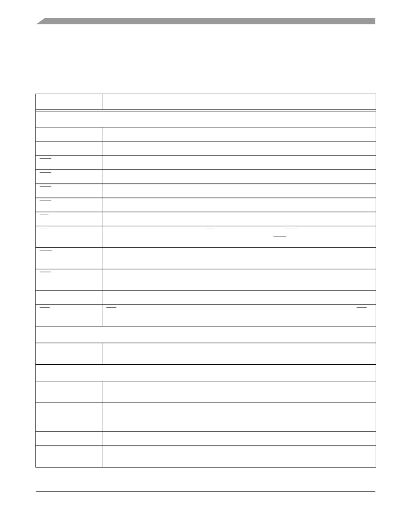
Signals and Connections
2 Signals and Connections
Table 3 identifies and describes the MC9328MX1 signals that are assigned to package pins. The signals are
grouped by the internal module that they are connected to.
Table 3. Signal Names and Descriptions
Signal Name
Function/Notes
External Bus/Chip Select (EIM)
A [24:0]
Address bus signals
D [31:0]
Data bus signals
EB0
MSB Byte Strobe—Active low external enable byte signal that controls D [31:24]
EB1
Byte Strobe—Active low external enable byte signal that controls D [23:16]
EB2
Byte Strobe—Active low external enable byte signal that controls D [15:8]
EB3
LSB Byte Strobe—Active low external enable byte signal that controls D [7:0]
OE
Memory Output Enable—Active low output enables external data bus
CS [5:0]
Chip Select—The chip select signals CS [3:2] are multiplexed with CSD [1:0] and are selected by
the Function Multiplexing Control Register (FMCR). By default CSD [1:0] is selected.
ECB
Active low input signal sent by flash device to the EIM whenever the flash device must terminate an
on-going burst sequence and initiate a new (long first access) burst sequence.
LBA
Active low signal sent by flash device causing the external burst device to latch the starting burst
address.
BCLK (burst clock)
Clock signal sent to external synchronous memories (such as burst flash) during burst mode.
RW
RW signal—Indicates whether external access is a read (high) or write (low) cycle. Used as a WE
input signal by external DRAM.
Bootstrap
BOOT [3:0]
System Boot Mode Select—The operational system boot mode of the MC9328MX1 upon system
reset is determined by the settings of these pins.
SDRAM Controller
SDBA [4:0]
SDRAM/SyncFlash non-interleave mode bank address multiplexed with address signals A [15:11].
These signals are logically equivalent to core address p_addr [25:21] in SDRAM/SyncFlash cycles.
SDIBA [3:0]
SDRAM/SyncFlash interleave addressing mode bank address multiplexed with address signals A
[19:16]. These signals are logically equivalent to core address p_addr [12:9] in SDRAM/SyncFlash
cycles.
MA [11:10]
SDRAM address signals
MA [9:0]
SDRAM address signals which are multiplex with address signals A [10:1]. MA [9:0] are selected on
SDRAM/SyncFlash cycles.
相關(guān)PDF資料 |
PDF描述 |
|---|---|
| MC68HC711E9CFN2 | Microcontrollers |
| MC68HC711E9CFN3 | Microcontrollers |
| MC68HC711E9CFS2 | Microcontrollers |
| MC68HC711E9CFS3 | Microcontrollers |
| MC68HC11A0CFN3 | HCMOS Single-Chip Microcontroller |
相關(guān)代理商/技術(shù)參數(shù) |
參數(shù)描述 |
|---|---|
| MC9328MX21CVM | 制造商:Freescale Semiconductor 功能描述:Microprocessor |
| MC9328MX21CVMR2 | 功能描述:處理器 - 專門應(yīng)用 DB I.MX21 17X17 PB-FR RoHS:否 制造商:Freescale Semiconductor 類型:Multimedia Applications 核心:ARM Cortex A9 處理器系列:i.MX6 數(shù)據(jù)總線寬度:32 bit 最大時(shí)鐘頻率:1 GHz 指令/數(shù)據(jù)緩存: 數(shù)據(jù) RAM 大小:128 KB 數(shù)據(jù) ROM 大小: 工作電源電壓: 最大工作溫度:+ 95 C 安裝風(fēng)格:SMD/SMT 封裝 / 箱體:MAPBGA-432 |
| MC9328MX21DVG | 制造商:Rochester Electronics LLC 功能描述:DB I.MX21 - Bulk 制造商:Motorola Inc 功能描述: 制造商:MOTOROLA 功能描述: |
| MC9328MX21DVGR2 | 制造商:Rochester Electronics LLC 功能描述:- Bulk |
| MC9328MX21DVH | 制造商:MOTOROLA 制造商全稱:Motorola, Inc 功能描述:i.MX family of microprocessors |
發(fā)布緊急采購,3分鐘左右您將得到回復(fù)。