- 您現(xiàn)在的位置:買賣IC網(wǎng) > PDF目錄371076 > MC908QL4C (Motorola, Inc.) Microcontrollers PDF資料下載
參數(shù)資料
| 型號: | MC908QL4C |
| 廠商: | Motorola, Inc. |
| 英文描述: | Microcontrollers |
| 中文描述: | 微控制器 |
| 文件頁數(shù): | 140/222頁 |
| 文件大小: | 2861K |
| 代理商: | MC908QL4C |
第1頁第2頁第3頁第4頁第5頁第6頁第7頁第8頁第9頁第10頁第11頁第12頁第13頁第14頁第15頁第16頁第17頁第18頁第19頁第20頁第21頁第22頁第23頁第24頁第25頁第26頁第27頁第28頁第29頁第30頁第31頁第32頁第33頁第34頁第35頁第36頁第37頁第38頁第39頁第40頁第41頁第42頁第43頁第44頁第45頁第46頁第47頁第48頁第49頁第50頁第51頁第52頁第53頁第54頁第55頁第56頁第57頁第58頁第59頁第60頁第61頁第62頁第63頁第64頁第65頁第66頁第67頁第68頁第69頁第70頁第71頁第72頁第73頁第74頁第75頁第76頁第77頁第78頁第79頁第80頁第81頁第82頁第83頁第84頁第85頁第86頁第87頁第88頁第89頁第90頁第91頁第92頁第93頁第94頁第95頁第96頁第97頁第98頁第99頁第100頁第101頁第102頁第103頁第104頁第105頁第106頁第107頁第108頁第109頁第110頁第111頁第112頁第113頁第114頁第115頁第116頁第117頁第118頁第119頁第120頁第121頁第122頁第123頁第124頁第125頁第126頁第127頁第128頁第129頁第130頁第131頁第132頁第133頁第134頁第135頁第136頁第137頁第138頁第139頁當前第140頁第141頁第142頁第143頁第144頁第145頁第146頁第147頁第148頁第149頁第150頁第151頁第152頁第153頁第154頁第155頁第156頁第157頁第158頁第159頁第160頁第161頁第162頁第163頁第164頁第165頁第166頁第167頁第168頁第169頁第170頁第171頁第172頁第173頁第174頁第175頁第176頁第177頁第178頁第179頁第180頁第181頁第182頁第183頁第184頁第185頁第186頁第187頁第188頁第189頁第190頁第191頁第192頁第193頁第194頁第195頁第196頁第197頁第198頁第199頁第200頁第201頁第202頁第203頁第204頁第205頁第206頁第207頁第208頁第209頁第210頁第211頁第212頁第213頁第214頁第215頁第216頁第217頁第218頁第219頁第220頁第221頁第222頁
Slave LIN Interface Controller (SLIC) Module
MC68HC908QL4 MC68HC908QL3 MC68HC908QL2 Data Sheet, Rev. 4
140
Freescale Semiconductor
IMSG — SLIC Ignore Message Bit
IMSG cannot be cleared by a write of 0, but is cleared automatically by the SLIC module after the next
BREAK/SYNC symbol pair is validated. After it is set, IMSG will not keep data from being written to the
receive data buffer, which means that the buffers cannot be assumed to contain known valid message
data until the next receive buffer full interrupt. IMSG must not be used in BTM mode.
1 = SLIC to ignore data field of message, SLIC interrupts are suppressed until the next message
header arrives
0 = Normal operation
SLCIE — SLIC Interrupt Enable
1 = SLIC interrupt sources are enabled
0 = SLIC interrupt sources are disabled
14.8.2 SLIC Control Register 2
SLIC control register 2 (SLCC2) contains bits used to control various features of the SLIC module.
SLCWCM — SLIC Wait Clock Mode
This bit can only be written once out of reset state.
1 = SLIC clocks stop when the CPU is placed into wait mode
0 = SLIC clocks continue to run when the CPU is placed into wait mode so that the SLIC can receive
messages and wakeup the CPU.
BTM — UART Byte Transfer Mode
Byte transmit mode bypasses the normal LIN message framing and checksum monitoring and allows
the user to send and receive single bytes in a method similar to a half-duplex UART. When enabled,
this mode reads the bit time register (SLCBT) value and assumes this is the value corresponding to
the number of SLIC clock counts for one bit time to establish the desired UART bit rate. The user
software must initialize this register prior to sending or receiving data, based on the input clock
selection, prescaler stage choice, and desired bit rate.
BTM forces the data length in SLCDLC to one byte (DLC = 0x00) and disables the checksum circuitry
so that CHKMOD has no effect. Refer to
14.9.15 Byte Transfer Mode Operation
for more detailed
information about how to use this mode. BTM sets up the SLIC module to send and receive one byte
at a time, with 8-bit data, no parity, and one stop bit (8-N-1). This is the most commonly used setup for
UART communications and should work for most applications. This is fixed in the SLIC and is not
configurable.
1 = UART byte transfer mode enabled
0 = UART byte transfer mode disabled
SLCE — SLIC Module Enable
1 = SLIC module enabled
0 = SLIC module disabled
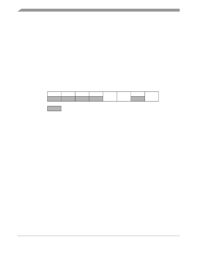
Bit 7
6
5
4
3
2
1
Bit 0
Read:
0
0
0
0
SLCWCM
BTM
0
SLCE
Write:
Reset:
0
0
0
0
0
0
0
0
= Unimplemented
Figure 14-5. SLIC Control Register 2 (SLCC2)
相關(guān)PDF資料 |
PDF描述 |
|---|---|
| MC908QL2C | Microcontrollers |
| MC908QL2DT | Microcontrollers |
| MC908QL2DW | Microcontrollers |
| MC908QL2M | Microcontrollers |
| MC908QL2V | Microcontrollers |
相關(guān)代理商/技術(shù)參數(shù) |
參數(shù)描述 |
|---|---|
| MC908QL4CDTE | 制造商:FREESCALE 制造商全稱:Freescale Semiconductor, Inc 功能描述:M68HC08 Microcontrollers |
| MC908QL4CDWE | 制造商:FREESCALE 制造商全稱:Freescale Semiconductor, Inc 功能描述:M68HC08 Microcontrollers |
| MC908QL4DT | 制造商:MOTOROLA 制造商全稱:Motorola, Inc 功能描述:Microcontrollers |
| MC908QL4DW | 制造商:MOTOROLA 制造商全稱:Motorola, Inc 功能描述:Microcontrollers |
| MC908QL4M | 制造商:MOTOROLA 制造商全稱:Motorola, Inc 功能描述:Microcontrollers |
發(fā)布緊急采購,3分鐘左右您將得到回復(fù)。