- 您現在的位置:買賣IC網 > PDF目錄11688 > MAX9273GTL/V+T (Maxim Integrated Products)IC SERIALIZER 22BIT GMSL 40TQFN PDF資料下載
參數資料
| 型號: | MAX9273GTL/V+T |
| 廠商: | Maxim Integrated Products |
| 文件頁數: | 49/49頁 |
| 文件大小: | 0K |
| 描述: | IC SERIALIZER 22BIT GMSL 40TQFN |
| 標準包裝: | 2,500 |
| 系列: | * |
第1頁第2頁第3頁第4頁第5頁第6頁第7頁第8頁第9頁第10頁第11頁第12頁第13頁第14頁第15頁第16頁第17頁第18頁第19頁第20頁第21頁第22頁第23頁第24頁第25頁第26頁第27頁第28頁第29頁第30頁第31頁第32頁第33頁第34頁第35頁第36頁第37頁第38頁第39頁第40頁第41頁第42頁第43頁第44頁第45頁第46頁第47頁第48頁當前第49頁
MAX9273
22-Bit GMSL Serializer with Coax or
STP Cable Drive
9
Maxim Integrated
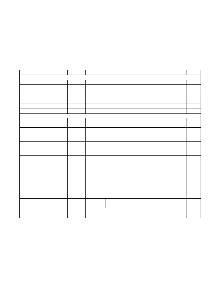
Note 2: To provide a midlevel, leave the input open, or, if driven, put driver in high impedance. High-impedance leakage current
must be less than Q10A.
Note 3: IIN min due to voltage drop across the internal pullup resistor.
Note 4: Specified pin to ground.
Note 5: Specified pin to all supply/ground.
Note 6: Guaranteed by design and not production tested.
Note 7: Measured in serial link bit times. Bit time = 1/(30 x fPCLKIN) for BWS = 0. Bit time = 1/(40 x fPCLKIN) for BWS = 1.
AC ELECTRICAL CHARACTERISTICS (continued)
(VDVDD = VAVDD = 1.7V to 1.9V, VIOVDD = 1.7V to 3.6V, RL = 100I Q1% (differential), EP connected to PCB ground (GND),
TA = -40NC to +105NC, unless otherwise noted. Typical values are at VDVDD = VAVDD = VIOVDD = 1.8V, TA = +25NC)
PARAMETER
SYMBOL
CONDITIONS
MIN
TYP
MAx
UNITS
I2C/UART and GPIO Port Timing
I2C/UART Bit Rate
9.6
1000
kbps
Output Rise Time
tR
30% to 70%, CL = 10pF to 100pF,
1kI pullup to IOVDD
20
120
ns
Output Fall Time
tF
70% to 30%, CL = 10pF to 100pF,
1kI pullup to IOVDD
20
120
ns
Input Setup Time
tSET
I2C only (Figure 6, Note 6)
100
ns
Input Hold Time
tHOLD
I2C only (Figure 6, Note 6)
0
ns
SWITCHING CHARACTERISTICS (Note 6)
Differential Output Rise/Fall
Time
tR, tF
20% to 80%, VOD R 400mV RL = 100I,
serial-bit rate = 1.5Gbps
250
ps
Total Serial Output Jitter
(Differential Output)
tTSOJ1
1.5Gbps PRBS signal, measured at
VOD = 0V differential, preemphasis
disabled (Figure 7)
0.25
UI
Deterministic Serial Output
Jitter (Differential Output)
tDSOJ2
1.5Gbps PRBS signal, measured at
VOD = 0V differential, preemphasis
disabled (Figure 7)
0.15
UI
Total Serial Output Jitter
(Single-Ended Output)
tTSOJ1
1.5Gbps PRBS signal, measured at VO/2,
preemphasis disabled (Figure 3)
0.25
UI
Deterministic Serial Output
Jitter (Single-Ended Output)
tDSOJ2
1.5Gbps PRBS signal, measured at VO/2,
preemphasis disabled (Figure 3)1.5Gbps
PRBS signal
0.15
UI
Parallel Data Input Setup Time
tSET
(Figure 8)
2
ns
Parallel Data Input Hold Time
tHOLD
(Figure 8)
1
ns
GPI-to-GPO Delay
tGPIO_
Deserializer GPI to serializer GPO
(Figure 9)
350
F
s
Serializer Delay (Note 7)
tSD
(Figure 10)
Spread spectrum enabled
6880
Bits
Spread spectrum disabled
3040
Link Start Time
tLOCK
(Figure 11)
2
ms
Power-Up Time
tPU
(Figure 12)
7
ms
相關PDF資料 |
PDF描述 |
|---|---|
| MAX9273GTL+T | IC SERIALIZER 22BIT GMSL 40TQFN |
| MAX9271GTJ/V+T | IC SERIALIZER 16BIT GMSL 32TQFN |
| VI-B3V-CU-S | CONVERTER MOD DC/DC 5.8V 200W |
| MAX9271GTJ+T | IC SERIALIZER 16BIT GMSL 32TQFN |
| VI-B3T-CU-S | CONVERTER MOD DC/DC 6.5V 200W |
相關代理商/技術參數 |
參數描述 |
|---|---|
| MAX9275GTN/V+T | 制造商:Maxim Integrated Products 功能描述:SERIALIZER WITH PARALLEL CMOS INPUTS, NON-HDCP - Tape and Reel |
| MAX9276GTN/V+GG6 | 制造商:Maxim Integrated Products 功能描述:IC DESERIALIZER GMSL 3.12GBPS |
| MAX9276GTN/V+T | 制造商:Maxim Integrated Products 功能描述:3.12GBPS GMSL DESERIALIZERS FOR COAX OR STP INPUTS AND PARAL - Tape and Reel |
| MAX9276GTN+ | 制造商:Maxim Integrated Products 功能描述:DE-SERIALIZER WITH PARALLEL CMOS OUTPUTS, NON-HDCP - Rail/Tube |
| MAX9277GTM/V+GG7 | 制造商:Maxim Integrated Products 功能描述:IC SERIALIZER LVDS |
發(fā)布緊急采購,3分鐘左右您將得到回復。