- 您現(xiàn)在的位置:買(mǎi)賣(mài)IC網(wǎng) > PDF目錄9782 > MAX9157EHJ+T (Maxim Integrated Products)IC TXRX QUAD LVDS 32-TQFP PDF資料下載
參數(shù)資料
| 型號(hào): | MAX9157EHJ+T |
| 廠商: | Maxim Integrated Products |
| 文件頁(yè)數(shù): | 9/16頁(yè) |
| 文件大?。?/td> | 0K |
| 描述: | IC TXRX QUAD LVDS 32-TQFP |
| 產(chǎn)品培訓(xùn)模塊: | Lead (SnPb) Finish for COTS Obsolescence Mitigation Program |
| 標(biāo)準(zhǔn)包裝: | 2,500 |
| 類(lèi)型: | 收發(fā)器 |
| 驅(qū)動(dòng)器/接收器數(shù): | 4/4 |
| 規(guī)程: | LVDS |
| 電源電壓: | 3 V ~ 3.6 V |
| 安裝類(lèi)型: | 表面貼裝 |
| 封裝/外殼: | 32-TQFP |
| 供應(yīng)商設(shè)備封裝: | 32-TQFP(5x5) |
| 包裝: | 帶卷 (TR) |
第1頁(yè)第2頁(yè)第3頁(yè)第4頁(yè)第5頁(yè)第6頁(yè)第7頁(yè)第8頁(yè)當(dāng)前第9頁(yè)第10頁(yè)第11頁(yè)第12頁(yè)第13頁(yè)第14頁(yè)第15頁(yè)第16頁(yè)
MAX9157
Quad Bus LVDS Transceiver
2
_______________________________________________________________________________________
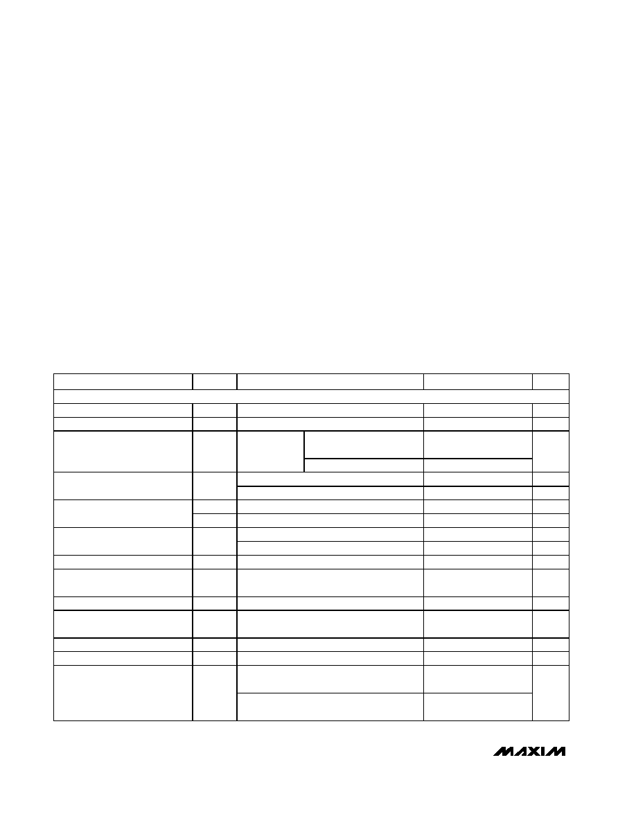
ABSOLUTE MAXIMUM RATINGS
DC ELECTRICAL CHARACTERISTICS
(VCC = 3.0V to 3.6V, RL = 27
±1%, differential input voltage |VID| = 0.1V to VCC, input common-mode voltage VCM = 0.05V to 2.4V,
input voltage range = 0 to VCC, DE_ = high, RE_ = low, TA = -40°C to +85°C, unless otherwise noted. Typical values are at VCC =
3.3V, |VID| = 0.2V, VCM = 1.2V, and TA = +25°C.) (Notes 1 and 2)
Stresses beyond those listed under “Absolute Maximum Ratings” may cause permanent damage to the device. These are stress ratings only, and functional
operation of the device at these or any other conditions beyond those indicated in the operational sections of the specifications is not implied. Exposure to
absolute maximum rating conditions for extended periods may affect device reliability.
VCC, AVCC to GND................................................-0.3V to +4.0V
DO_+/RIN_+, DO_-/RIN_-, to GND .......................-0.3V to +4.0V
DIN_, DE_, RE_ to GND.........................................-0.3V to +4.0V
RO_ to GND................................................-0.3V to (VCC + 0.3V)
AGND to GND .......................................................-0.3V to +0.3V
Short-Circuit Duration (DO_+/RIN_+, DO_-/RIN_-) ....Continuous
Continuous Power Dissipation (TA = +70°C)
MAX9157EGJ (derate 21.2mW/°C above +70°C) .....1702mW
MAX9157EHJ (derate 11.1mW/°C above +70°C).........889mW
Storage Temperature Range .............................-65°C to +150°C
Maximum Junction Temperature .....................................+150°C
Operating Temperature Range ...........................-40°C to +85°C
ESD Protection
Human Body Model (DO_+/RIN_+, DO_-/RIN_-).............±4kV
Lead Temperature (soldering, 10s) .................................+300°C
PARAMETER
SYMBOL
CONDITIONS
MIN
TYP
MAX
UNITS
BLVDS (DO_+/RIN_+, DO_-/RIN_-)
Differential Input High Threshold
VTH
DE_ = low
26
100
mV
Differential Input Low Threshold
VTL
DE_ = low
-100
-26
mV
TA = +25
°C, VCC = 3.3V,
VCM = 1.2V
12
26
43
Threshold Hysteresis (Note 3)
VHYST
DE_ = low
Full operating range
9
26
78
mV
0.1V
≤VID≤ 0.6V, DE_ = low
-15
±1.8
15
A
Input Current
IIN+, IIN-
0.6V
< VID≤ 1.2V, DE_ = low
-20
±2.5
20
A
RIN1
VCC = 3.6V, 0 or open, Figure 1
53
k
Input Resistance
RIN2
VCC = 3.6V, 0 or open, Figure 1
148
k
0.1V
≤ VID≤ 0.6V, VCC = 0 or open
-15
±0.9
15
A
Power-Off Input Current
IINO+,
IINO-
0.6V
< VID≤ 1.2V, VCC = 0 or open
-20
±1.8
20
A
Differential Output Voltage
VOD
Figure 2
250
405
460
mV
Change in Magnitude of VOD for
Complementary Output States
VOD
Figure 2
1
25
mV
Offset Voltage
VOS
Figure 2
1.185
1.302
1.435
V
Change in Magnitude of VOS for
Complementary Output States
VOS
Figure 2
3.3
25
mV
Output High Voltage
VOH
Figure 2
1.505
1.6
V
Output Low Voltage
VOL
Figure 2
0.9
1.099
V
DIN_ = high, DO_+/RIN_+ = 0 or
VCC, DO_-/RIN_- = 0 or VCC
-30
-14.8
30
Output Short-Circuit Current
IOS
DIN_ = low, DO_-/RIN_- = 0 or
VCC, DO_+/RIN_+ = 0 or VCC
-30
-14.8
30
mA
相關(guān)PDF資料 |
PDF描述 |
|---|---|
| MS27472E18A35P | CONN RCPT 66POS WALL MNT W/PINS |
| MS27656E25A29P | CONN RCPT 29POS WALL MNT W/PINS |
| VI-2NM-IU-F2 | CONVERTER MOD DC/DC 10V 200W |
| VI-JTL-MW-B1 | CONVERTER MOD DC/DC 28V 100W |
| MS3116J8-2P | CONN PLUG 2POS STRAIGHT W/PINS |
相關(guān)代理商/技術(shù)參數(shù) |
參數(shù)描述 |
|---|---|
| MAX9158 | 制造商:MAXIM 制造商全稱(chēng):Maxim Integrated Products 功能描述:Quad Bus LVDS Transceiver in 44 QFN |
| MAX9158EGM | 制造商:Maxim Integrated Products 功能描述:QUAD BUS LVDS TRANSCEIVER IN 44-PIN QFN - Rail/Tube 制造商:Rochester Electronics LLC 功能描述: |
| MAX9158EGM-T | 制造商:Maxim Integrated Products 功能描述:QUAD BUS LVDS TRANSCEIVER IN 44-PIN QFN - Tape and Reel |
| MAX9159 | 制造商:MAXIM 制造商全稱(chēng):Maxim Integrated Products 功能描述:Dual LVDS Line Receiver |
| MAX9159ESA | 制造商:Maxim Integrated Products 功能描述:DUAL LVDS LINE RECEIVER - Rail/Tube |
發(fā)布緊急采購(gòu),3分鐘左右您將得到回復(fù)。