- 您現(xiàn)在的位置:買(mǎi)賣(mài)IC網(wǎng) > PDF目錄9814 > MAX9121EUE+T (Maxim Integrated Products)IC RCVR QUAD LVDS 16-TSSOP PDF資料下載
參數(shù)資料
| 型號(hào): | MAX9121EUE+T |
| 廠商: | Maxim Integrated Products |
| 文件頁(yè)數(shù): | 5/12頁(yè) |
| 文件大小: | 0K |
| 描述: | IC RCVR QUAD LVDS 16-TSSOP |
| 產(chǎn)品培訓(xùn)模塊: | Lead (SnPb) Finish for COTS Obsolescence Mitigation Program |
| 標(biāo)準(zhǔn)包裝: | 2,500 |
| 類(lèi)型: | 接收器 |
| 驅(qū)動(dòng)器/接收器數(shù): | 0/4 |
| 規(guī)程: | LVDS |
| 電源電壓: | 3 V ~ 3.6 V |
| 安裝類(lèi)型: | 表面貼裝 |
| 封裝/外殼: | 16-TSSOP(0.173",4.40mm 寬) |
| 供應(yīng)商設(shè)備封裝: | 16-TSSOP |
| 包裝: | 帶卷 (TR) |
VCC to GND ...........................................................-0.3V to +4.0V
IN_+, IN_- to GND .................................................-0.3V to +4.0V
EN, EN to GND ...........................................-0.3V to (VCC + 0.3V)
OUT_ to GND .............................................-0.3V to (VCC + 0.3V)
Continuous Power Dissipation (TA = +70°C)
16-Pin TSSOP (derate 9.4mW/°C above +70°C) .........755mW
16-Pin SO (derate 8.7mW/°C above +70°C)................696mW
Storage Temperature Range .............................-65°C to +150°C
Maximum Junction Temperature .....................................+150°C
Operating Temperature Range ...........................-40°C to +85°C
Lead Temperature (soldering, 10s) .................................+300°C
ESD Protection
(Human Body Model, IN_+, IN_-) ....................................±8kV
MAX9121/MAX9122
Quad LVDS Line Receivers with
Integrated Termination and Flow-Through Pinout
2
_______________________________________________________________________________________
ABSOLUTE MAXIMUM RATINGS
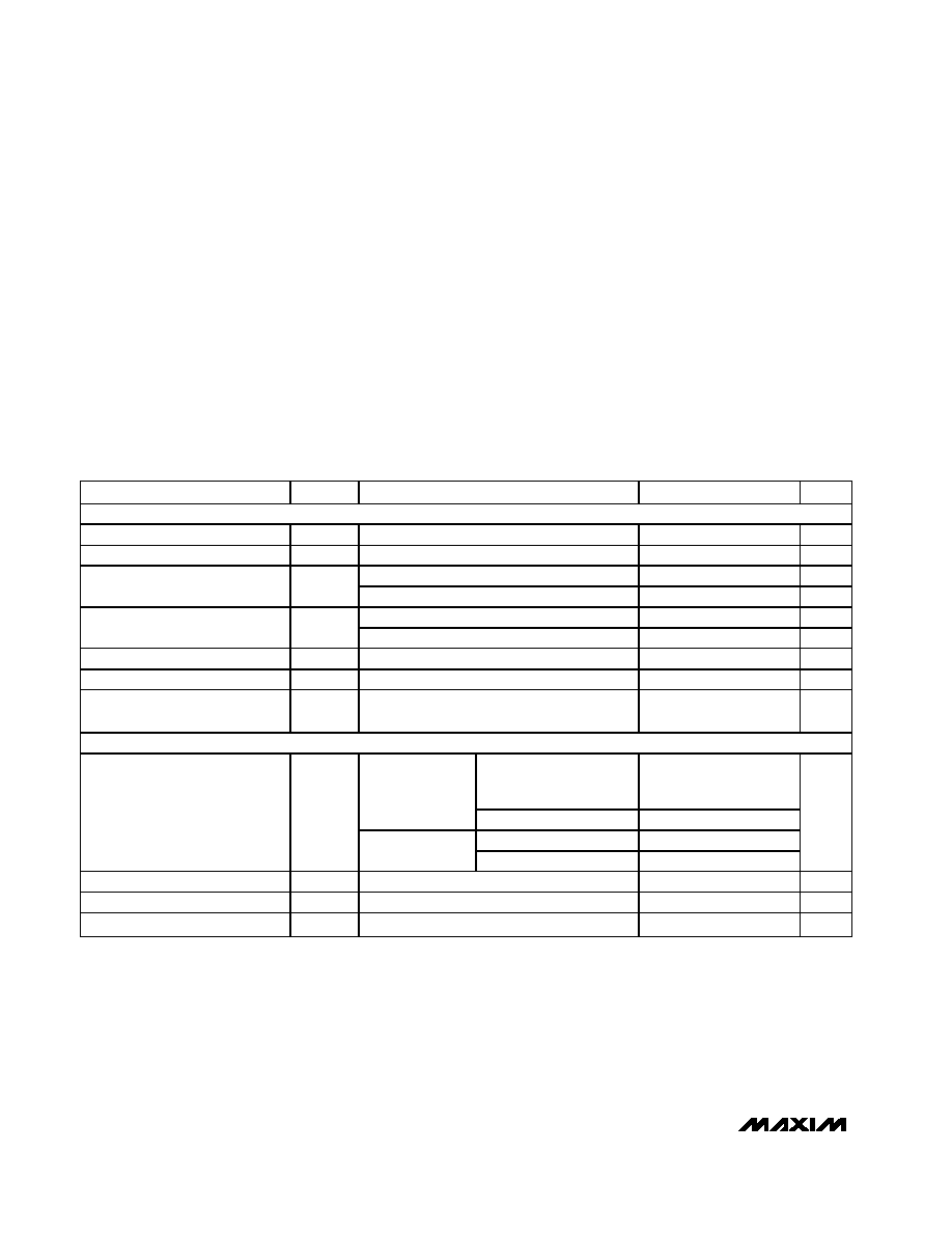
DC ELECTRICAL CHARACTERISTICS
(VCC = +3.0V to +3.6V, differential input voltage |VID| = 0.1V to 1.0V, common-mode voltage VCM = |VID/2| to 2.4V - |VID/2|,
TA = -40°C to +85°C. Typical values are at VCC = +3.3V, TA = +25°C, unless otherwise noted.) (Note 1)
Stresses beyond those listed under “Absolute Maximum Ratings” may cause permanent damage to the device. These are stress ratings only, and functional
operation of the device at these or any other conditions beyond those indicated in the operational sections of the specifications is not implied. Exposure to
absolute maximum rating conditions for extended periods may affect device reliability.
PARAMETER
SYMBOL
CONDITIONS
MIN
TYP
MAX
UNITS
LVDS INPUTS (IN_+, IN_-)
Differential Input High Threshold
VTH
100
mV
Differential Input Low Threshold
VTL
-100
mV
0.1V
≤VID≤ 0.6V
-20
20
A
Input Current (MAX9121)
IIN_+, IIN_-
0.6V
<VID≤ 1.0V
-25
25
A
0.1V
≤VID≤ 0.6V, VCC = 0
-20
20
A
Power-Off Input Current
(MAX9121)
IINOFF
0.6V <
VID≤ 1.0V, VCC = 0
-25
25
A
Input Resistor 1
RIN1
VCC = 3.6V or 0, Figure 1
35
k
Input Resistor 2
RIN2
VCC = 3.6V or 0, Figure 1
132
k
Differential Input Resistance
(MAX9122)
RDIFF
VCC = 3.6V or 0, Figure 1
90
107
132
LVCMOS/LVTTL OUTPUTS (OUT_)
Open, undriven short, or
undriven 100
parallel
termination
2.7
3.2
IOH = -4.0mA
(MAX9121)
VID = +100mV
2.7
3.2
Open or undriven short
2.7
3.2
Output High Voltage (Table 1)
VOH
IOH = -4.0mA
(MAX9122)
VID = +100mV
2.7
3.2
V
Output Low Voltage
VOL
IOL = +4.0mA, VID = -100mV
0.1
0.25
V
Output Short-Circuit Current
IOS
Enabled, VID = 0.1V, VOUT_ = 0 (Note 2)
-15
-120
mA
Output High-Impedance Current
IOZ
Disabled, VOUT = 0 or VCC
-10
+10
A
相關(guān)PDF資料 |
PDF描述 |
|---|---|
| VI-J6X-MX-F2 | CONVERTER MOD DC/DC 5.2V 75W |
| MAX9124ESE+T | IC DRVR QUAD LVDS 16-SOIC |
| MS27656E13B8PB | CONN RCPT 8POS WALL MNT W/PINS |
| MAX3486ESA+T | IC TXRX RS485/422 2.5MBPS 8SOIC |
| MS27497T8F98PA | CONN RCPT 3POS WALL MNT W/PINS |
相關(guān)代理商/技術(shù)參數(shù) |
參數(shù)描述 |
|---|---|
| MAX9121EVKIT | 功能描述:LVDS 接口集成電路 Evaluation Kit for the MAX9121 MAX9122 MAX9123 RoHS:否 制造商:Texas Instruments 激勵(lì)器數(shù)量:4 接收機(jī)數(shù)量:4 數(shù)據(jù)速率:155.5 Mbps 工作電源電壓:5 V 最大功率耗散:1025 mW 最大工作溫度:+ 85 C 封裝 / 箱體:SOIC-16 Narrow 封裝:Reel |
| MAX9122 | 制造商:MAXIM 制造商全稱:Maxim Integrated Products 功能描述:Quad LVDS Line Receivers with Integrated Termination and Flow-Through Pinout |
| MAX9122ESE | 制造商:Maxim Integrated Products 功能描述:QUAD LVDS LINE RECEIVER WITH INTEGRATED TERMI - Bulk 制造商:Rochester Electronics LLC 功能描述: |
| MAX9122ESE+ | 制造商:Maxim Integrated Products 功能描述:LINE RCVR 4RX 16SOIC N - Bulk |
| MAX9122ESE+T | 制造商:Maxim Integrated Products 功能描述:LINE RCVR 4RX 16SOIC N - Tape and Reel |
發(fā)布緊急采購(gòu),3分鐘左右您將得到回復(fù)。