- 您現(xiàn)在的位置:買賣IC網(wǎng) > PDF目錄385527 > MAX3774 (Maxim Integrated Products, Inc.) Dual-Rate Fibre Channel Repeaters PDF資料下載
參數(shù)資料
| 型號(hào): | MAX3774 |
| 廠商: | Maxim Integrated Products, Inc. |
| 英文描述: | Dual-Rate Fibre Channel Repeaters |
| 中文描述: | 雙速率的光纖通道中繼器 |
| 文件頁(yè)數(shù): | 2/9頁(yè) |
| 文件大小: | 220K |
| 代理商: | MAX3774 |
M
Dual-Rate Fibre Channel Repeaters
2
_______________________________________________________________________________________
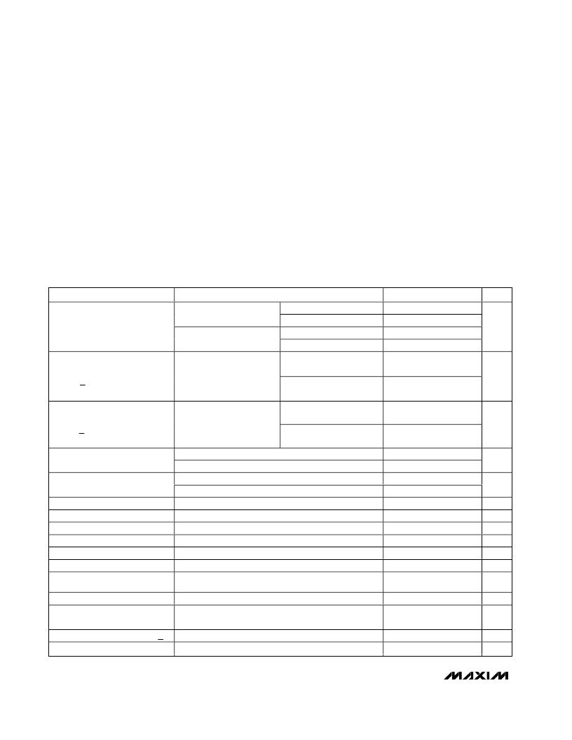
ABSOLUTE MAXIMUM RATINGS
V
CC
........................................................................-0.5V to +5.0V
Pin Voltage Levels (IN±, CF±,
RATESEL, CLKEN, LOCK) .....................-0.5V to (V
CC
+ 0.5V)
Current into LOCK...............................................-1mA to +10mA
CML Output Currents (OUT±, CLK±), R
OUT
= 75
........ +22mA
CML Output Currents (OUT±, CLK±), R
OUT
= 50
........ +33mA
ELECTRICAL CHARACTERISTICS
(V
CC
= +3.0V to +3.6V, 8B/10B data coding, C
F
= 0.047μF, lock pin loaded with
≥
15k
resistor, all high-speed inputs and outputs
AC-coupled, T
A
= 0
°
C to +70
°
C, unless otherwise noted. Typical values are at V
CC
= +3.3V, T
A
= +25
°
C.)
Stresses beyond those listed under “Absolute Maximum Ratings” may cause permanent damage to the device. These are stress ratings only, and functional
operation of the device at these or any other conditions beyond those indicated in the operational sections of the specifications is not implied. Exposure to
absolute maximum rating conditions for extended periods may affect device reliability.
Continuous Power Dissipation (T
A
= +70
°
C)
16-Pin QSOP-EP (derate 18.9mW/
°
C above +70
°
C)...702mW
Operating Junction Temperature Range...........-55
°
C to +150
°
C
Operating Temperature Range .........................-55
°
C to +110
°
C
Storage Temperature Range ............................-55
°
C to +150
°
C
Lead Temperature (soldering, 10s) ................................+300
°
C
PARAMETER
CONDITIONS
MIN
80
68
115
95
TYP
101
88
146
121
MAX
140
124
195
164
UNITS
MAX3772/MAX3773
MAX3774/MAX3775
MAX3772/MAX3773
MAX3774/MAX3775
CLKEN = GND
Supply Current (Note 1)
CLKEN = V
CC
mA
MAX3772/MAX3773,
100
terminated
1000
1400
1800
Differential Voltage Signal
at OUT
Figure 1
MAX3774/MAX3775,
150
terminated
1000
1400
1800
mVp-p
MAX3772/MAX3773
100
terminated
MAX3774/MAX3775,
150
terminated
1000
1400
1800
Differential Voltage Signal
at CLK
Figure 1
1000
1400
1800
mVp-p
1.0625Gbps operation, RATESEL = GND
2.125Gbps operation, RATESEL = V
CC
20% to 80% 1.0625Gbps operation
20% to 80% 2.125Gbps operation
20% to 80% (Note 2)
20% to 80% (Note 2)
I
OL
= +250μA (sinking)
I
OH
= -100μA (sourcing)
-100
-100
136
75
100
50
+100
+100
325
160
175
100
0.4
Input Data Rate Range
ppm
Input Edge Speed
ps
Data Transition Time (OUT±)
Clock Transition Time (CLK±)
LOCK Output Low
LOCK Output High
CLKEN, RATESEL Input Current
CLKEN, RATESEL Input Low
130
75
ps
ps
V
V
μA
V
2.4
-50
-0.3
50
0.8
V
CC
+ 0.3
2200
CLKEN, RATESEL Input High
2
V
Differential Input Voltage Swing
200
mVp-p
Input Common-Mode Voltage
V
CC
-
0.45
V
Differential Voltage across CF
CDR Lock Time
(Note 2)
Input = CJTPAT (Note 3)
V
CC
V
μs
500
相關(guān)PDF資料 |
PDF描述 |
|---|---|
| MAX3775 | Dual-Rate Fibre Channel Repeaters |
| MAX3772 | Quad LVDS Transmitter with Flow-Through Pinout 16-TSSOP -40 to 85 |
| MAX3772CEE | Replaced by SN65LVDS048A : LVDS Quad Differential Line Receiver 16-SOIC -40 to 85 |
| MAX3773CEE | Replaced by SN65LVDS048A : LVDS Quad Differential Line Receiver 16-TSSOP -40 to 85 |
| MAX3775CEE | Quad LVDS Receiver with Flow-Through Pinout 16-SOIC -40 to 85 |
相關(guān)代理商/技術(shù)參數(shù) |
參數(shù)描述 |
|---|---|
| MAX3774CEE | 制造商:Rochester Electronics LLC 功能描述: 制造商:Maxim Integrated Products 功能描述: |
| MAX3774CEE+T | 制造商:Maxim Integrated Products 功能描述:- Tape and Reel |
| MAX3775CEE+T | 制造商:Maxim Integrated Products 功能描述:- Tape and Reel |
| MAX3780EVKIT | 制造商:Maxim Integrated Products 功能描述:QUAD 2.5GBPS CABLE TRANSCEIVER - Rail/Tube |
| MAX3781EVKIT | 功能描述:交換機(jī) IC 開發(fā)工具 RoHS:否 制造商:Maxim Integrated 產(chǎn)品:Evaluation Kits 類型:USB Power Switches 工具用于評(píng)估:MAX4984E 工作電源電壓:2.8 V to 5.5 V |
發(fā)布緊急采購(gòu),3分鐘左右您將得到回復(fù)。