- 您現(xiàn)在的位置:買賣IC網(wǎng) > PDF目錄45048 > M38C59GFHP 8-BIT, OTPROM, 6.25 MHz, MICROCONTROLLER, PQFP80 PDF資料下載
參數(shù)資料
| 型號: | M38C59GFHP |
| 元件分類: | 微控制器/微處理器 |
| 英文描述: | 8-BIT, OTPROM, 6.25 MHz, MICROCONTROLLER, PQFP80 |
| 封裝: | 12 X 12 MM, 0.50 MM PITCH, PLASTIC, LQFP-80 |
| 文件頁數(shù): | 36/71頁 |
| 文件大?。?/td> | 939K |
| 代理商: | M38C59GFHP |
第1頁第2頁第3頁第4頁第5頁第6頁第7頁第8頁第9頁第10頁第11頁第12頁第13頁第14頁第15頁第16頁第17頁第18頁第19頁第20頁第21頁第22頁第23頁第24頁第25頁第26頁第27頁第28頁第29頁第30頁第31頁第32頁第33頁第34頁第35頁當(dāng)前第36頁第37頁第38頁第39頁第40頁第41頁第42頁第43頁第44頁第45頁第46頁第47頁第48頁第49頁第50頁第51頁第52頁第53頁第54頁第55頁第56頁第57頁第58頁第59頁第60頁第61頁第62頁第63頁第64頁第65頁第66頁第67頁第68頁第69頁第70頁第71頁
Rev.2.00
Nov 23, 2005
page 41 of 75
REJ03B0098-0200
38C5 Group (One Time PROM version)
A/D CONVERTER
The 38C5 group has a 10-bit A/D converter. The A/D converter per-
forms successive approximation conversion.The 38C5 group has the
ADKEY function which perform A/D conversion of the “L” level ana-
log input from the ADKEY pin automatically.
[AD Conversion Register (ADL, ADH)]
One of these registers is a high-order register, and the other is a low-
order register. The high-order 8 bits of a conversion result is stored in
the AD conversion register (high-order) (address 001716), and the
low-order 2 bits of the same result are stored in bit 7 and bit 6 of the
AD conversion register (low-order) (address 001616).
During A/D conversion, do not read these registers.
Also, the connection between the resistor ladder and reference volt-
age input pin (VREF) can be controlled by the VREF input switch bit (bit
0 of address 001616). When “1” is written to this bit, the resistor ladder
is always connected to VREF. When “0” is written to this bit, the resistor
ladder is disconnected from VREF except during the A/D conversion.
[AD Control Register (ADCON)]
This register controls A/D converter. Bits 2 to 0 are analog input pin
selection bits. Bit 3 is an AD conversion completion bit and “0” during A/
D conversion. This bit is set to “1” upon completion of A/D conversion.
A/D conversion is started by setting “0” in this bit.
Bit 5 is the ADKEY enable bit. The ADKEY function is enabled by
setting “1” to this bit. When this function is valid, the analog input
selection bit is ignored. Also, when bit 5 is “1”, do not set “0” to bit 3
by program.
[Comparison Voltage Generator]
The comparison voltage generator divides the voltage between AVSS
and VREF, and outputs the divided voltages.
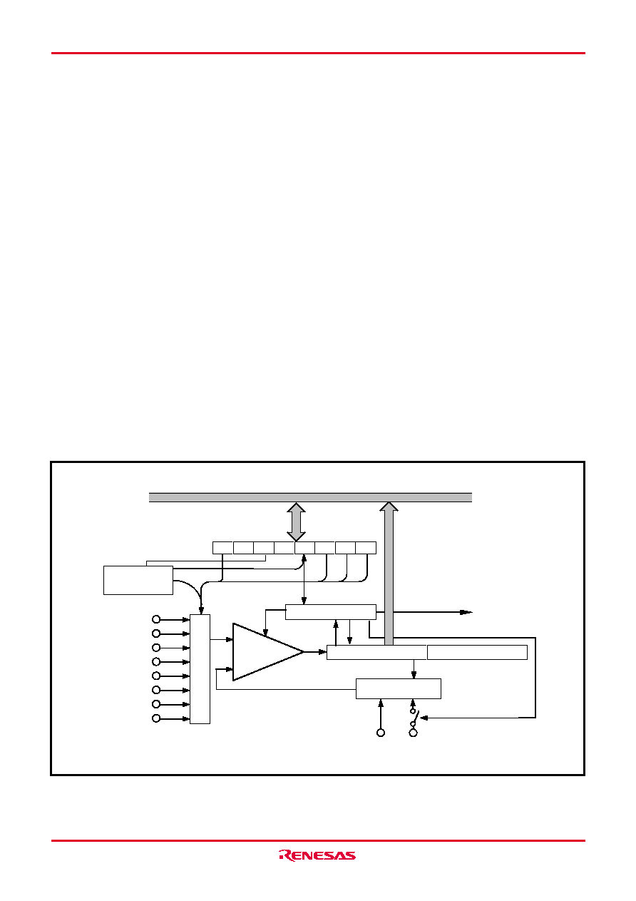
Fig. 38 Block diagram of A/D converter
ADKEY
control circuit
AVSS
VREF
b7b0
P50/AN0
P51/AN1
P52/AN2
P53/AN3
P54/AN4
P55/AN5
P56/AN6
P57/AN7/ADKEY0
Data bus
A/D interrupt request
AD control register
C
h
a
n
e
l
s
e
le
c
to
r
Comparator
A/D control circuit
AD conversion register (H) AD conversion register (L)
(Address 001716)
(Address 001616)
Resistor ladder
[Channel Selector]
The channel selector selects one of the input ports P57/AN7–P50/
AN0 and inputs it to the comparator.
[Comparator and Control Circuit]
The comparator and control circuit compare an analog input voltage
with the comparison voltage and store the result in the AD conver-
sion register. When an A/D conversion is completed, the control cir-
cuit sets the AD conversion completion bit and the AD conversion
interrupt request bit to “1.”
The comparator is constructed linked to a capacitor. The conversion
accuracy may be low because the change is lost if the conversion
speed is not enough.
Accordingly, set f(XIN) to at least 500 kHz during A/D conversion in
the middle- or high- speed mode.
Also, do not execute the STP and WIT instructions during the A/D
conversion.
In the low-speed mode, since the A/D conversion is executed by the
built-in self-oscillation circuit, the minimum value of f(XIN) frequency.
相關(guān)PDF資料 |
PDF描述 |
|---|---|
| M38C89EFFP | 8-BIT, OTPROM, 4 MHz, MICROCONTROLLER, PQFP144 |
| M38C89MF-XXXFP | 8-BIT, MROM, 4 MHz, MICROCONTROLLER, PQFP144 |
| M38C89EFFP | 8-BIT, OTPROM, 4 MHz, MICROCONTROLLER, PQFP144 |
| M38C89MF-XXXFP | 8-BIT, MROM, 4 MHz, MICROCONTROLLER, PQFP144 |
| M38C89EFFP | 8-BIT, OTPROM, 4 MHz, MICROCONTROLLER, PQFP144 |
相關(guān)代理商/技術(shù)參數(shù) |
參數(shù)描述 |
|---|---|
| M38C59GFHP#U0 | 制造商:Renesas Electronics Corporation 功能描述:MCU 2/4V 60K PB-FREE - Trays |
| M38D20F1XXXFP | 制造商:RENESAS 制造商全稱:Renesas Technology Corp 功能描述:SINGLE-CHIP 8-BIT CMOS MICROCOMPUTER |
| M38D20F1XXXHP | 制造商:RENESAS 制造商全稱:Renesas Technology Corp 功能描述:SINGLE-CHIP 8-BIT CMOS MICROCOMPUTER |
| M38D20F2XXXFP | 制造商:RENESAS 制造商全稱:Renesas Technology Corp 功能描述:SINGLE-CHIP 8-BIT CMOS MICROCOMPUTER |
| M38D20F2XXXHP | 制造商:RENESAS 制造商全稱:Renesas Technology Corp 功能描述:SINGLE-CHIP 8-BIT CMOS MICROCOMPUTER |
發(fā)布緊急采購,3分鐘左右您將得到回復(fù)。