- 您現(xiàn)在的位置:買賣IC網(wǎng) > PDF目錄45048 > M38C59GFHP 8-BIT, OTPROM, 6.25 MHz, MICROCONTROLLER, PQFP80 PDF資料下載
參數(shù)資料
| 型號: | M38C59GFHP |
| 元件分類: | 微控制器/微處理器 |
| 英文描述: | 8-BIT, OTPROM, 6.25 MHz, MICROCONTROLLER, PQFP80 |
| 封裝: | 12 X 12 MM, 0.50 MM PITCH, PLASTIC, LQFP-80 |
| 文件頁數(shù): | 25/71頁 |
| 文件大小: | 939K |
| 代理商: | M38C59GFHP |
第1頁第2頁第3頁第4頁第5頁第6頁第7頁第8頁第9頁第10頁第11頁第12頁第13頁第14頁第15頁第16頁第17頁第18頁第19頁第20頁第21頁第22頁第23頁第24頁當前第25頁第26頁第27頁第28頁第29頁第30頁第31頁第32頁第33頁第34頁第35頁第36頁第37頁第38頁第39頁第40頁第41頁第42頁第43頁第44頁第45頁第46頁第47頁第48頁第49頁第50頁第51頁第52頁第53頁第54頁第55頁第56頁第57頁第58頁第59頁第60頁第61頁第62頁第63頁第64頁第65頁第66頁第67頁第68頁第69頁第70頁第71頁
Rev.2.00
Nov 23, 2005
page 31 of 75
REJ03B0098-0200
38C5 Group (One Time PROM version)
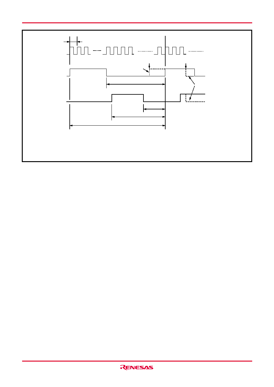
Fig. 26 Waveform of PWM/IGBT
s Notes on Timer X
(1) Write Order to Timer X
In the timer mode, pulse output mode, event counter mode and
pulse width measurement mode, write to the following registers in
the order as shown below;
the timer X register (extension),
the timer X register (low-order),
the timer X register (high-order).
Do not write to only one of them.
When the above mode is set and timer X operates as the 16-bit
counter, if the timer X register (extension) is never set after reset is
released, setting the timer X register (extension) is not required. In
this case, write the timer X register (low-order) first and the timer X
register (high-order). However, once writing to the timer X register
(extension) is executed, note that the value is retained to the reload
latch.
In the IGBT output and PWM modes, do not write “1” to the timer X
register (extension). Also, when “1” is already written to the timer X
register, be sure to write “0” to the register before using.
Write to the following registers in the order as shown below;
the compare registers 1, 2, 3 (high- and low-order),
the timer X register (extension),
the timer X register (low-order),
the timer X register (high-order).
It is possible to use whichever order to write to the compare regis-
ters 1, 2, 3 (high- and low-order). However, write both the compare
registers 1, 2, 3 and the timer X register at the same time.
(2) Read Order to Timer X
In all modes, read the following registers in the order as shown below;
the timer X register (extension),
the timer X register (high-order),
the timer X register (low-order).
When reading the timer X register (extension) is not required, read
the timer X register (high-order) first and the timer X register (low-
order).
Read order to the compare registers 1, 2, 3 is not specified.
Write to or read from the timer X register by the 16-bit unit. If read-
ing to the timer X register during write operation or writing to it dur-
ing read operation is performed, normal operation will not be per-
formed.
(3) Write to Timer X
Which write control can be selected by the timer X write control bit
(b3) of the timer X mode register (address 2D16), writing data to
both the latch and the timer at the same time or writing data only to
the latch. When writing a value to the timer X address to write to the
latch only, the value is set into the reload latch and the timer is
updated at the next underflow. After reset release, when writing a
value to the timer X address, the value is set into the timer and the
timer latch at the same time, because they are written at the same
time.
When writing to the latch only, if the write timing to the high-order
reload latch and the underflow timing are almost the same, the value
is set into the timer and the timer latch at the same time. In this time,
counting is stopped during writing to the high-order reload latch.
Do not switch the timer count source during timer count operation.
Stop the timer count before switching it.
ts
Timer X count source
Timer X PWM mode
IGBT output mode
m ts
(n+1) ts
TXOUT1 output
(TXCON1 bit 5 = “1”)
TXOUT2 output
(TXCON2 bit 1 = “0”)
q ts
p ts
n : Timer X setting value
m: Compare register 1 setting value
p : Compare register 2 setting value
q : Compare register 3 setting value
ts: One period of timer X count source
External trigger (INT0 source)
is generated.
INT1 or INT2 source is generated.
Level is “H” only IGBT
output mode.
The following PWM waveform is output;
Duty of TXOUT1 output :{(n+1)-m}/(n+1),
Duty of TXOUT2 output :(p-q)/(n+1),
Period :(n+1) ts
Level is forcibly “L” only IGBT output mode.
相關PDF資料 |
PDF描述 |
|---|---|
| M38C89EFFP | 8-BIT, OTPROM, 4 MHz, MICROCONTROLLER, PQFP144 |
| M38C89MF-XXXFP | 8-BIT, MROM, 4 MHz, MICROCONTROLLER, PQFP144 |
| M38C89EFFP | 8-BIT, OTPROM, 4 MHz, MICROCONTROLLER, PQFP144 |
| M38C89MF-XXXFP | 8-BIT, MROM, 4 MHz, MICROCONTROLLER, PQFP144 |
| M38C89EFFP | 8-BIT, OTPROM, 4 MHz, MICROCONTROLLER, PQFP144 |
相關代理商/技術參數(shù) |
參數(shù)描述 |
|---|---|
| M38C59GFHP#U0 | 制造商:Renesas Electronics Corporation 功能描述:MCU 2/4V 60K PB-FREE - Trays |
| M38D20F1XXXFP | 制造商:RENESAS 制造商全稱:Renesas Technology Corp 功能描述:SINGLE-CHIP 8-BIT CMOS MICROCOMPUTER |
| M38D20F1XXXHP | 制造商:RENESAS 制造商全稱:Renesas Technology Corp 功能描述:SINGLE-CHIP 8-BIT CMOS MICROCOMPUTER |
| M38D20F2XXXFP | 制造商:RENESAS 制造商全稱:Renesas Technology Corp 功能描述:SINGLE-CHIP 8-BIT CMOS MICROCOMPUTER |
| M38D20F2XXXHP | 制造商:RENESAS 制造商全稱:Renesas Technology Corp 功能描述:SINGLE-CHIP 8-BIT CMOS MICROCOMPUTER |
發(fā)布緊急采購,3分鐘左右您將得到回復。