- 您現(xiàn)在的位置:買賣IC網(wǎng) > PDF目錄45046 > M38507F8FP 8-BIT, MROM, 8 MHz, MICROCONTROLLER, PDSO42 PDF資料下載
參數(shù)資料
| 型號(hào): | M38507F8FP |
| 元件分類: | 微控制器/微處理器 |
| 英文描述: | 8-BIT, MROM, 8 MHz, MICROCONTROLLER, PDSO42 |
| 封裝: | 0.450 INCH, 0.80 MM PITCH, PLASTIC, SSOP-42 |
| 文件頁數(shù): | 242/287頁 |
| 文件大?。?/td> | 2969K |
| 代理商: | M38507F8FP |
第1頁第2頁第3頁第4頁第5頁第6頁第7頁第8頁第9頁第10頁第11頁第12頁第13頁第14頁第15頁第16頁第17頁第18頁第19頁第20頁第21頁第22頁第23頁第24頁第25頁第26頁第27頁第28頁第29頁第30頁第31頁第32頁第33頁第34頁第35頁第36頁第37頁第38頁第39頁第40頁第41頁第42頁第43頁第44頁第45頁第46頁第47頁第48頁第49頁第50頁第51頁第52頁第53頁第54頁第55頁第56頁第57頁第58頁第59頁第60頁第61頁第62頁第63頁第64頁第65頁第66頁第67頁第68頁第69頁第70頁第71頁第72頁第73頁第74頁第75頁第76頁第77頁第78頁第79頁第80頁第81頁第82頁第83頁第84頁第85頁第86頁第87頁第88頁第89頁第90頁第91頁第92頁第93頁第94頁第95頁第96頁第97頁第98頁第99頁第100頁第101頁第102頁第103頁第104頁第105頁第106頁第107頁第108頁第109頁第110頁第111頁第112頁第113頁第114頁第115頁第116頁第117頁第118頁第119頁第120頁第121頁第122頁第123頁第124頁第125頁第126頁第127頁第128頁第129頁第130頁第131頁第132頁第133頁第134頁第135頁第136頁第137頁第138頁第139頁第140頁第141頁第142頁第143頁第144頁第145頁第146頁第147頁第148頁第149頁第150頁第151頁第152頁第153頁第154頁第155頁第156頁第157頁第158頁第159頁第160頁第161頁第162頁第163頁第164頁第165頁第166頁第167頁第168頁第169頁第170頁第171頁第172頁第173頁第174頁第175頁第176頁第177頁第178頁第179頁第180頁第181頁第182頁第183頁第184頁第185頁第186頁第187頁第188頁第189頁第190頁第191頁第192頁第193頁第194頁第195頁第196頁第197頁第198頁第199頁第200頁第201頁第202頁第203頁第204頁第205頁第206頁第207頁第208頁第209頁第210頁第211頁第212頁第213頁第214頁第215頁第216頁第217頁第218頁第219頁第220頁第221頁第222頁第223頁第224頁第225頁第226頁第227頁第228頁第229頁第230頁第231頁第232頁第233頁第234頁第235頁第236頁第237頁第238頁第239頁第240頁第241頁當(dāng)前第242頁第243頁第244頁第245頁第246頁第247頁第248頁第249頁第250頁第251頁第252頁第253頁第254頁第255頁第256頁第257頁第258頁第259頁第260頁第261頁第262頁第263頁第264頁第265頁第266頁第267頁第268頁第269頁第270頁第271頁第272頁第273頁第274頁第275頁第276頁第277頁第278頁第279頁第280頁第281頁第282頁第283頁第284頁第285頁第286頁第287頁
HARDWARE
3850 Group (Spec. H) User’s Manual
FUNCTIONAL DESCRIPTION
1-40
Flash Memory Mode
The M38507F8 (flash memory version) has an internal new DINOR
(DIvided bit line NOR) flash memory that can be rewritten with a
single power source when VCC is 5 V, and 2 power sources when
VCC is 3.3-5.0 V.
For this flash memory , three flash memory modes are available in
which to read, program, and erase: parallel I/O and standard serial I/
O modes in which the flash memory can be manipulated using a
programmer and a CPU rewrite mode in which the flash memory can
be manipulated by the Central Processing Unit (CPU). Each mode is
detailed in the pages to follow.
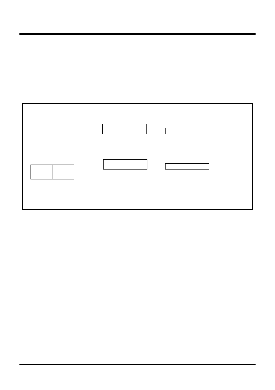
Fig. 44 Block diagram of flash memory version
The flash memory of the M38507F8 is divided into User ROM area
and Boot ROM area as shown in Figure 44.
In addition to the ordinary user ROM area to store a microcomputer
operation control program, the flash memory has a Boot ROM area
that is used to store a program to control rewriting in CPU rewrite
and standard serial I/O modes. This Boot ROM area has had a stan-
dard serial I/O mode control program stored in it when shipped from
the factory. However, the user can write a rewrite control program in
this area that suits the user’s application system. This Boot ROM
area can be rewritten in only parallel I/O mode.
800016
Block 1 : 32 kbyte
User ROM area
4 kbyte
F00016
FFFF16
Boot ROM area
Notes 1: The Boot ROM area can be rewritten in only parallel
input/output mode. (Access to any other areas is inhibited.)
2: To specify a block, use the maximum address in the block.
Product name
Flash memory
start address
M38507F8800016
Parallel I/O mode
800016
Block 1 : 32 kbyte
FFFF16
CPU rewrite mode, standard serial I/O mode
User ROM area
4 kbyte
F00016
FFFF16
Boot ROM area
BSEL = 0BSEL = 1
User area / Boot area selection bit = 0
User area / Boot area selection bit = 1
相關(guān)PDF資料 |
PDF描述 |
|---|---|
| M38504E6FP | 8-BIT, MROM, 8 MHz, MICROCONTROLLER, PDSO42 |
| M38504E6SP | 8-BIT, MROM, 8 MHz, MICROCONTROLLER, PDIP42 |
| M38504M6-XXXSP | 8-BIT, MROM, 8 MHz, MICROCONTROLLER, PDIP42 |
| M38504M6-XXXFP | 8-BIT, MROM, 8 MHz, MICROCONTROLLER, PDSO42 |
| M38503M4H-XXXFP | 8-BIT, MROM, 8 MHz, MICROCONTROLLER, PDSO42 |
相關(guān)代理商/技術(shù)參數(shù) |
參數(shù)描述 |
|---|---|
| M38507F8FP#U1 | 制造商:Renesas Electronics Corporation 功能描述:MCU 8BIT 740 CISC 32KB FLASH 5V 42SSOP - Trays |
| M38507F8FP#W1 | 制造商:Renesas Electronics Corporation 功能描述:FLASH 8-BIT 2.7 TO 5.5V PBFREE |
| M38507F8FP(#U1) | 制造商:Renesas Electronics Corporation 功能描述: |
| M3851 BK001 | 制造商:Alpha Wire Company 功能描述:CBL 7COND 14AWG BLK 1000' |
| M3851 BK002 | 制造商:Alpha Wire Company 功能描述:CBL 7COND 14AWG BLK 500' |
發(fā)布緊急采購,3分鐘左右您將得到回復(fù)。