- 您現(xiàn)在的位置:買賣IC網(wǎng) > PDF目錄45044 > M38222M2DXXXGP 8-BIT, MROM, 4 MHz, MICROCONTROLLER, PQFP80 PDF資料下載
參數(shù)資料
| 型號: | M38222M2DXXXGP |
| 元件分類: | 微控制器/微處理器 |
| 英文描述: | 8-BIT, MROM, 4 MHz, MICROCONTROLLER, PQFP80 |
| 封裝: | 14 X 14 MM, PLASTIC, QFP-80 |
| 文件頁數(shù): | 259/328頁 |
| 文件大?。?/td> | 2300K |
| 代理商: | M38222M2DXXXGP |
第1頁第2頁第3頁第4頁第5頁第6頁第7頁第8頁第9頁第10頁第11頁第12頁第13頁第14頁第15頁第16頁第17頁第18頁第19頁第20頁第21頁第22頁第23頁第24頁第25頁第26頁第27頁第28頁第29頁第30頁第31頁第32頁第33頁第34頁第35頁第36頁第37頁第38頁第39頁第40頁第41頁第42頁第43頁第44頁第45頁第46頁第47頁第48頁第49頁第50頁第51頁第52頁第53頁第54頁第55頁第56頁第57頁第58頁第59頁第60頁第61頁第62頁第63頁第64頁第65頁第66頁第67頁第68頁第69頁第70頁第71頁第72頁第73頁第74頁第75頁第76頁第77頁第78頁第79頁第80頁第81頁第82頁第83頁第84頁第85頁第86頁第87頁第88頁第89頁第90頁第91頁第92頁第93頁第94頁第95頁第96頁第97頁第98頁第99頁第100頁第101頁第102頁第103頁第104頁第105頁第106頁第107頁第108頁第109頁第110頁第111頁第112頁第113頁第114頁第115頁第116頁第117頁第118頁第119頁第120頁第121頁第122頁第123頁第124頁第125頁第126頁第127頁第128頁第129頁第130頁第131頁第132頁第133頁第134頁第135頁第136頁第137頁第138頁第139頁第140頁第141頁第142頁第143頁第144頁第145頁第146頁第147頁第148頁第149頁第150頁第151頁第152頁第153頁第154頁第155頁第156頁第157頁第158頁第159頁第160頁第161頁第162頁第163頁第164頁第165頁第166頁第167頁第168頁第169頁第170頁第171頁第172頁第173頁第174頁第175頁第176頁第177頁第178頁第179頁第180頁第181頁第182頁第183頁第184頁第185頁第186頁第187頁第188頁第189頁第190頁第191頁第192頁第193頁第194頁第195頁第196頁第197頁第198頁第199頁第200頁第201頁第202頁第203頁第204頁第205頁第206頁第207頁第208頁第209頁第210頁第211頁第212頁第213頁第214頁第215頁第216頁第217頁第218頁第219頁第220頁第221頁第222頁第223頁第224頁第225頁第226頁第227頁第228頁第229頁第230頁第231頁第232頁第233頁第234頁第235頁第236頁第237頁第238頁第239頁第240頁第241頁第242頁第243頁第244頁第245頁第246頁第247頁第248頁第249頁第250頁第251頁第252頁第253頁第254頁第255頁第256頁第257頁第258頁當前第259頁第260頁第261頁第262頁第263頁第264頁第265頁第266頁第267頁第268頁第269頁第270頁第271頁第272頁第273頁第274頁第275頁第276頁第277頁第278頁第279頁第280頁第281頁第282頁第283頁第284頁第285頁第286頁第287頁第288頁第289頁第290頁第291頁第292頁第293頁第294頁第295頁第296頁第297頁第298頁第299頁第300頁第301頁第302頁第303頁第304頁第305頁第306頁第307頁第308頁第309頁第310頁第311頁第312頁第313頁第314頁第315頁第316頁第317頁第318頁第319頁第320頁第321頁第322頁第323頁第324頁第325頁第326頁第327頁第328頁
1-21
SINGLE-CHIP 8-BIT CMOS MICROCOMPUTER
MITSUBISHI MICROCOMPUTERS
3822 Group
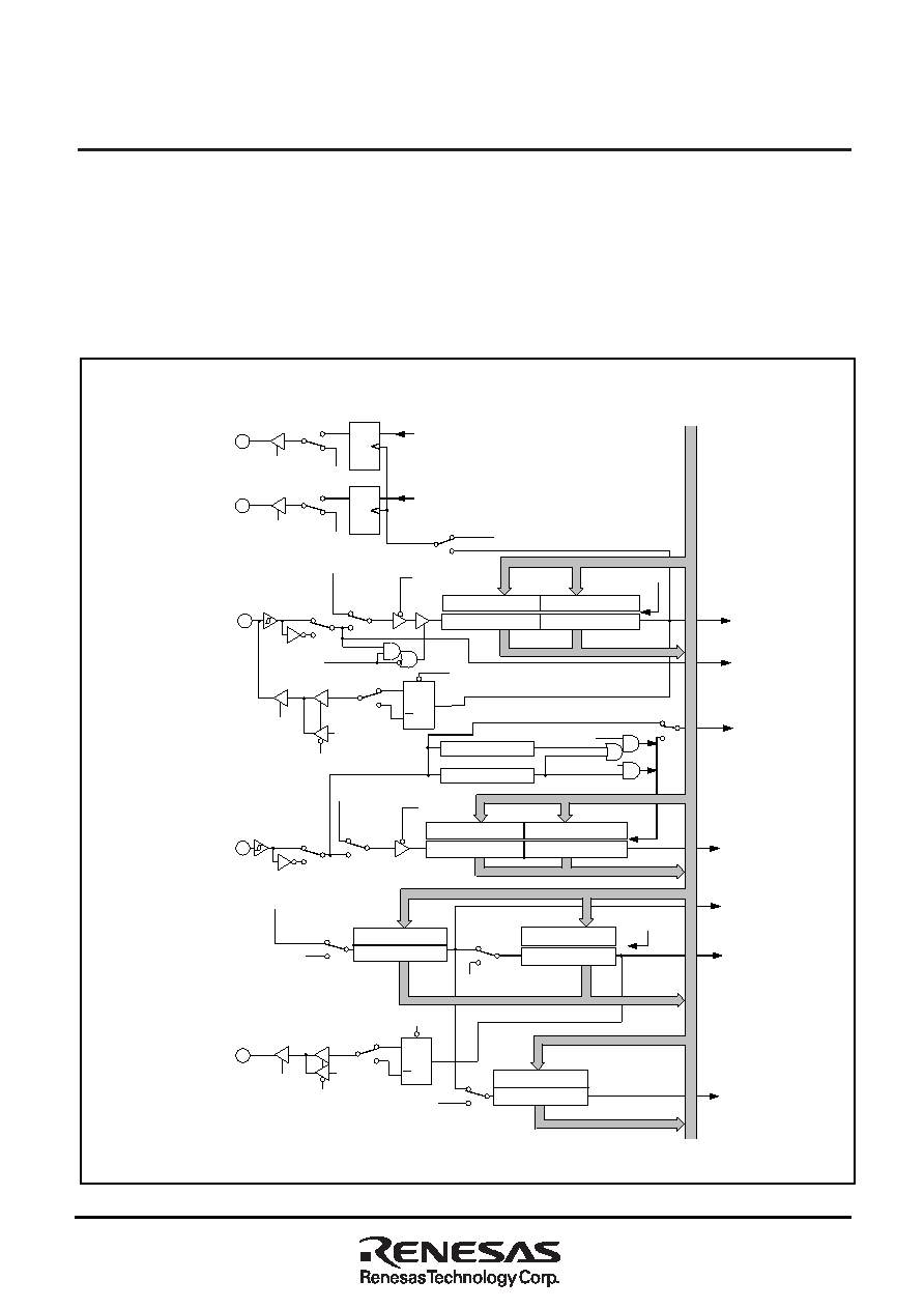
TIMERS
The 3822 group has five timers: timer X, timer Y, timer 1, timer 2,
and timer 3. Timer X and timer Y are 16-bit timers, and timer 1,
timer 2, and timer 3 are 8-bit timers.
All timers are down count timers. When the timer reaches “0016”,
an underflow occurs at the next count pulse and the correspond-
ing timer latch is reloaded into the timer and the count is contin-
ued. When a timer underflows, the interrupt request bit corre-
sponding to that timer is set to “1”.
Read and write operation on 16-bit timer must be performed for
both high and low-order bytes. When reading a 16-bit timer, read
the high-order byte first. When writing to a 16-bit timer, write the
low-order byte first. The 16-bit timer cannot perform the correct op-
eration when reading during the write operation, or when writing
during the read operation.
Fig. 17 Timer block diagram
CNTR0 active
edge switch bit
Timer 1 count source
selection bit
Real time port
control bit “0”
“1”
P55/CNTR1
“0”
f(XIN)/16
(f(XCIN)/16 in low-speed modeV)
CNTR1 active
edge switch bit
“10”
Timer Y stop
control bit
Falling edge detection
Period
measurement mode
Timer Y
interrupt
request
Pulse width HL continuously measurement mode
Rising edge detection
“00”,“01”,“11”
Timer Y operating
mode bit
Timer X
interrupt
request
Timer X mode register
write signal
P54/CNTR0
Q
T
S
P54 direction register
Pulse output mode
P54 latch
Timer X stop
control bit
“0”
“1”
Timer X write
control bit
Q D
Latch
Q D
Latch
“1”
“0”
“1”
“10”
Timer X operat-
ing mode bit
“00”,“01”,“11”
f(XIN)/16
(f(XCIN)/16 in low-speed modeV)
Pulse width
measurement
mode
CNTR0 active
edge switch bit
Pulse output mode
Q
T
S
“0”
P56 direction register
P56 latch
“1”
TOUT output
active edge
switch bit “0”
Timer 2 write
control bit
“0”
“1”
TOUT output
control bit
“1”
P56/TOUT
XCIN
Timer 3 count
source selection bit
“0”
“1”
Timer 2
interrupt
request
Timer 3
interrupt
request
TOUT output control bit
Timer 2 count source
selection bit
Timer 1
interrupt
request
Data bus
f(XIN)/16
(f(XCIN)/16 in low-speed modeV)
f(XIN)/16
(f(XCIN)/16 in low-speed modeV)
f(XIN)/16(f(XCIN)/16 in low-speed modeV)
VInternal clock
φ = XCIN/2.
CNTR0
interrupt
request
CNTR1
interrupt
request
Timer Y operating mode bit
“00”,“01”,“10”
“11”
P60 direction register “0”
Real time port
control bit “1”
P60
P60 latch
P61 direction register “0”
Real time port
control bit “1”
P61
P61 latch
P60 data for real time port
P61 data for real time port
Timer Y (low) (8)
Timer Y (high) (8)
Timer 3 latch (8)
Timer 3 (8)
Timer 1 latch (8)
Timer 1 (8)
Timer 2 latch (8)
Timer 2 (8)
Timer X (low) (8)
Timer X (high) (8)
Timer X (low) latch (8)
Timer X (high) latch (8)
Timer Y (low) latch (8)
Timer Y (high) latch (8)
相關PDF資料 |
PDF描述 |
|---|---|
| M38223E4-XXXGP | 8-BIT, OTPROM, 4 MHz, MICROCONTROLLER, PQFP80 |
| M38223E4FS | 8-BIT, OTPROM, 4 MHz, MICROCONTROLLER, CQCC80 |
| M38227ECFP | 8-BIT, OTPROM, 4 MHz, MICROCONTROLLER, PQFP80 |
| M38223M4HXXXFP | 8-BIT, MROM, 4 MHz, MICROCONTROLLER, PQFP80 |
| M38223E4GP | 8-BIT, OTPROM, 4 MHz, MICROCONTROLLER, PQFP80 |
相關代理商/技術參數(shù) |
參數(shù)描述 |
|---|---|
| M38223E4FS | 制造商:Renesas Electronics Corporation 功能描述:MCU 8BIT 740 CISC 16KB EPROM 5V 80CLCC - Bulk |
| M38223M4148FP | 制造商:Renesas Electronics Corporation 功能描述:M16C FLASH 256K/20K, 24MHZ,DMA,I2C,IEBU - Trays |
| M38223M4A-123FP#UO | 制造商:Renesas Electronics Corporation 功能描述: |
| M38223M4A-159HP#U0 | 制造商:Renesas Electronics Corporation 功能描述: |
| M38224M6A-376HP#U0 | 制造商:Renesas Electronics Corporation 功能描述: |
發(fā)布緊急采購,3分鐘左右您將得到回復。