- 您現(xiàn)在的位置:買賣IC網(wǎng) > PDF目錄385509 > M38207M8-117HP (Mitsubishi Electric Corporation) 1 watt dc-dc converters PDF資料下載
參數(shù)資料
| 型號(hào): | M38207M8-117HP |
| 廠商: | Mitsubishi Electric Corporation |
| 元件分類: | DC/DC變換器 |
| 英文描述: | 1 watt dc-dc converters |
| 中文描述: | 1瓦的DC - DC轉(zhuǎn)換器 |
| 文件頁數(shù): | 195/344頁 |
| 文件大?。?/td> | 5067K |
| 代理商: | M38207M8-117HP |
第1頁第2頁第3頁第4頁第5頁第6頁第7頁第8頁第9頁第10頁第11頁第12頁第13頁第14頁第15頁第16頁第17頁第18頁第19頁第20頁第21頁第22頁第23頁第24頁第25頁第26頁第27頁第28頁第29頁第30頁第31頁第32頁第33頁第34頁第35頁第36頁第37頁第38頁第39頁第40頁第41頁第42頁第43頁第44頁第45頁第46頁第47頁第48頁第49頁第50頁第51頁第52頁第53頁第54頁第55頁第56頁第57頁第58頁第59頁第60頁第61頁第62頁第63頁第64頁第65頁第66頁第67頁第68頁第69頁第70頁第71頁第72頁第73頁第74頁第75頁第76頁第77頁第78頁第79頁第80頁第81頁第82頁第83頁第84頁第85頁第86頁第87頁第88頁第89頁第90頁第91頁第92頁第93頁第94頁第95頁第96頁第97頁第98頁第99頁第100頁第101頁第102頁第103頁第104頁第105頁第106頁第107頁第108頁第109頁第110頁第111頁第112頁第113頁第114頁第115頁第116頁第117頁第118頁第119頁第120頁第121頁第122頁第123頁第124頁第125頁第126頁第127頁第128頁第129頁第130頁第131頁第132頁第133頁第134頁第135頁第136頁第137頁第138頁第139頁第140頁第141頁第142頁第143頁第144頁第145頁第146頁第147頁第148頁第149頁第150頁第151頁第152頁第153頁第154頁第155頁第156頁第157頁第158頁第159頁第160頁第161頁第162頁第163頁第164頁第165頁第166頁第167頁第168頁第169頁第170頁第171頁第172頁第173頁第174頁第175頁第176頁第177頁第178頁第179頁第180頁第181頁第182頁第183頁第184頁第185頁第186頁第187頁第188頁第189頁第190頁第191頁第192頁第193頁第194頁當(dāng)前第195頁第196頁第197頁第198頁第199頁第200頁第201頁第202頁第203頁第204頁第205頁第206頁第207頁第208頁第209頁第210頁第211頁第212頁第213頁第214頁第215頁第216頁第217頁第218頁第219頁第220頁第221頁第222頁第223頁第224頁第225頁第226頁第227頁第228頁第229頁第230頁第231頁第232頁第233頁第234頁第235頁第236頁第237頁第238頁第239頁第240頁第241頁第242頁第243頁第244頁第245頁第246頁第247頁第248頁第249頁第250頁第251頁第252頁第253頁第254頁第255頁第256頁第257頁第258頁第259頁第260頁第261頁第262頁第263頁第264頁第265頁第266頁第267頁第268頁第269頁第270頁第271頁第272頁第273頁第274頁第275頁第276頁第277頁第278頁第279頁第280頁第281頁第282頁第283頁第284頁第285頁第286頁第287頁第288頁第289頁第290頁第291頁第292頁第293頁第294頁第295頁第296頁第297頁第298頁第299頁第300頁第301頁第302頁第303頁第304頁第305頁第306頁第307頁第308頁第309頁第310頁第311頁第312頁第313頁第314頁第315頁第316頁第317頁第318頁第319頁第320頁第321頁第322頁第323頁第324頁第325頁第326頁第327頁第328頁第329頁第330頁第331頁第332頁第333頁第334頁第335頁第336頁第337頁第338頁第339頁第340頁第341頁第342頁第343頁第344頁
APPLICATION
2.5 Serial I/O1
3820 GROUP USER’S MANUAL
2–109
I
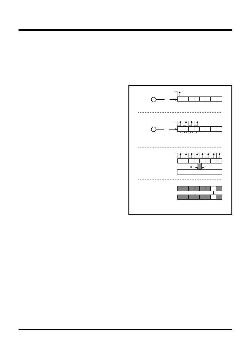
Receive operation in the clock synchronous mode
Receive operation in the clock synchronous mode is described below.
G
Start of receive operation
A receive operation is started by writing the following data into the receive buffer register (address
0018
16
) in the receive enable state.
8
1
Transmit data in the full duplex data transfer mode
Arbitrary dummy data in the half duplex data transfer mode
G
Receive operation
Each 1-bit data is read into the receive shift
register from the P4
4
/RxD pin in synchroni-
zation with the rising of the shift clocks.
The data enters first into the most significant
bit of the receive shift register. Each time 1-
bit data is received, the data of the receive
shift register is shifted by 1 bit toward the
least significant bit.
When 1-byte data has been input into the
receive shift register, the data of the receive
shift register is transferred to the receive buffer
register (address 0018
16
).
8
2
When a data transfer to the receive buffer
register is completed, the receive buffer full
flag (bit 1) of the serial I/O1 status register
(address 0019
16
) is set to “1,”
8
3
a serial I/O1
receive interrupt request occurs.
8
1: Initialization of register or others for a re-
ceive operation. Refer to
“2.5.4 Register
setting example.”
8
2: When data remains without reading out the data of the receive buffer register (the receive buffer
full flag is “1”) and yet all the receive data has been input to the receive shift register, the overrun
error flag of the serial I/O1 status register is set to “1.” At this time, the data of the receive shift
register is not transferred to the receive buffer register, but the former data of the receive buffer
register is held.
8
3: The receive buffer full flag is cleared to “0” by reading out the receive buffer register.
Receive shift register
P4
4
/RxD
D
1
b0
D
0
Receive shift register
b0
D
4
P4
4
/RxD
D
3
D
0
D
1
D
2
Transfer receive data
[Address 18
16
]
Receive buffer register
Receive shift register
D
7
D
4
D
5
D
6
Serial I/O1 status
register
[Address 19
16
]
b1
0
1
D
3
D
0
D
1
D
2
相關(guān)PDF資料 |
PDF描述 |
|---|---|
| M38B43MCH-XXXXFP | SINGLE-CHIP 8-BIT CMOS MICROCOMPUTER |
| M464S6453CKS | PC133/PC100 SODIMM |
| M5-D2 | Adjustable Type Coils |
| M5-F1 | Adjustable Type Coils |
| M5-H1 | Adjustable Type Coils |
相關(guān)代理商/技術(shù)參數(shù) |
參數(shù)描述 |
|---|---|
| M38207M8-501FP | 制造商:Mitsubishi Electric 功能描述:MicroController, 8-Bit, 80 Pin, Plastic, QFP 制造商:Renesas Electronics Corporation 功能描述:MicroController, 8-Bit, 80 Pin, Plastic, QFP |
| M38207M8-516HP | 制造商:Renesas Electronics Corporation 功能描述:MicroController, 8-Bit, 80 Pin, Plastic, QFP 制造商:VeriFone 功能描述:MicroController, 8-Bit, 80 Pin, Plastic, QFP |
| M38207RFS | 制造商:Renesas Electronics Corporation 功能描述:EMULATION MCU/8BIT CMOS EMULATION CHIP - Bulk |
| M3821 BK001 | 制造商:Alpha Wire 功能描述:CBL 25COND 18AWG BLK 1000' |
| M3821 BK002 | 制造商:Alpha Wire 功能描述:CBL 25COND 18AWG BLK 500' |
發(fā)布緊急采購(gòu),3分鐘左右您將得到回復(fù)。