- 您現(xiàn)在的位置:買賣IC網(wǎng) > PDF目錄98006 > M37721S2BFP 16-BIT, MICROCONTROLLER, PQFP100 PDF資料下載
參數(shù)資料
| 型號: | M37721S2BFP |
| 元件分類: | 微控制器/微處理器 |
| 英文描述: | 16-BIT, MICROCONTROLLER, PQFP100 |
| 封裝: | 14 X 20 MM, 0.65 MM PITCH, PLASTIC, QFP-100 |
| 文件頁數(shù): | 210/576頁 |
| 文件大小: | 6745K |
| 代理商: | M37721S2BFP |
第1頁第2頁第3頁第4頁第5頁第6頁第7頁第8頁第9頁第10頁第11頁第12頁第13頁第14頁第15頁第16頁第17頁第18頁第19頁第20頁第21頁第22頁第23頁第24頁第25頁第26頁第27頁第28頁第29頁第30頁第31頁第32頁第33頁第34頁第35頁第36頁第37頁第38頁第39頁第40頁第41頁第42頁第43頁第44頁第45頁第46頁第47頁第48頁第49頁第50頁第51頁第52頁第53頁第54頁第55頁第56頁第57頁第58頁第59頁第60頁第61頁第62頁第63頁第64頁第65頁第66頁第67頁第68頁第69頁第70頁第71頁第72頁第73頁第74頁第75頁第76頁第77頁第78頁第79頁第80頁第81頁第82頁第83頁第84頁第85頁第86頁第87頁第88頁第89頁第90頁第91頁第92頁第93頁第94頁第95頁第96頁第97頁第98頁第99頁第100頁第101頁第102頁第103頁第104頁第105頁第106頁第107頁第108頁第109頁第110頁第111頁第112頁第113頁第114頁第115頁第116頁第117頁第118頁第119頁第120頁第121頁第122頁第123頁第124頁第125頁第126頁第127頁第128頁第129頁第130頁第131頁第132頁第133頁第134頁第135頁第136頁第137頁第138頁第139頁第140頁第141頁第142頁第143頁第144頁第145頁第146頁第147頁第148頁第149頁第150頁第151頁第152頁第153頁第154頁第155頁第156頁第157頁第158頁第159頁第160頁第161頁第162頁第163頁第164頁第165頁第166頁第167頁第168頁第169頁第170頁第171頁第172頁第173頁第174頁第175頁第176頁第177頁第178頁第179頁第180頁第181頁第182頁第183頁第184頁第185頁第186頁第187頁第188頁第189頁第190頁第191頁第192頁第193頁第194頁第195頁第196頁第197頁第198頁第199頁第200頁第201頁第202頁第203頁第204頁第205頁第206頁第207頁第208頁第209頁當(dāng)前第210頁第211頁第212頁第213頁第214頁第215頁第216頁第217頁第218頁第219頁第220頁第221頁第222頁第223頁第224頁第225頁第226頁第227頁第228頁第229頁第230頁第231頁第232頁第233頁第234頁第235頁第236頁第237頁第238頁第239頁第240頁第241頁第242頁第243頁第244頁第245頁第246頁第247頁第248頁第249頁第250頁第251頁第252頁第253頁第254頁第255頁第256頁第257頁第258頁第259頁第260頁第261頁第262頁第263頁第264頁第265頁第266頁第267頁第268頁第269頁第270頁第271頁第272頁第273頁第274頁第275頁第276頁第277頁第278頁第279頁第280頁第281頁第282頁第283頁第284頁第285頁第286頁第287頁第288頁第289頁第290頁第291頁第292頁第293頁第294頁第295頁第296頁第297頁第298頁第299頁第300頁第301頁第302頁第303頁第304頁第305頁第306頁第307頁第308頁第309頁第310頁第311頁第312頁第313頁第314頁第315頁第316頁第317頁第318頁第319頁第320頁第321頁第322頁第323頁第324頁第325頁第326頁第327頁第328頁第329頁第330頁第331頁第332頁第333頁第334頁第335頁第336頁第337頁第338頁第339頁第340頁第341頁第342頁第343頁第344頁第345頁第346頁第347頁第348頁第349頁第350頁第351頁第352頁第353頁第354頁第355頁第356頁第357頁第358頁第359頁第360頁第361頁第362頁第363頁第364頁第365頁第366頁第367頁第368頁第369頁第370頁第371頁第372頁第373頁第374頁第375頁第376頁第377頁第378頁第379頁第380頁第381頁第382頁第383頁第384頁第385頁第386頁第387頁第388頁第389頁第390頁第391頁第392頁第393頁第394頁第395頁第396頁第397頁第398頁第399頁第400頁第401頁第402頁第403頁第404頁第405頁第406頁第407頁第408頁第409頁第410頁第411頁第412頁第413頁第414頁第415頁第416頁第417頁第418頁第419頁第420頁第421頁第422頁第423頁第424頁第425頁第426頁第427頁第428頁第429頁第430頁第431頁第432頁第433頁第434頁第435頁第436頁第437頁第438頁第439頁第440頁第441頁第442頁第443頁第444頁第445頁第446頁第447頁第448頁第449頁第450頁第451頁第452頁第453頁第454頁第455頁第456頁第457頁第458頁第459頁第460頁第461頁第462頁第463頁第464頁第465頁第466頁第467頁第468頁第469頁第470頁第471頁第472頁第473頁第474頁第475頁第476頁第477頁第478頁第479頁第480頁第481頁第482頁第483頁第484頁第485頁第486頁第487頁第488頁第489頁第490頁第491頁第492頁第493頁第494頁第495頁第496頁第497頁第498頁第499頁第500頁第501頁第502頁第503頁第504頁第505頁第506頁第507頁第508頁第509頁第510頁第511頁第512頁第513頁第514頁第515頁第516頁第517頁第518頁第519頁第520頁第521頁第522頁第523頁第524頁第525頁第526頁第527頁第528頁第529頁第530頁第531頁第532頁第533頁第534頁第535頁第536頁第537頁第538頁第539頁第540頁第541頁第542頁第543頁第544頁第545頁第546頁第547頁第548頁第549頁第550頁第551頁第552頁第553頁第554頁第555頁第556頁第557頁第558頁第559頁第560頁第561頁第562頁第563頁第564頁第565頁第566頁第567頁第568頁第569頁第570頁第571頁第572頁第573頁第574頁第575頁第576頁
7721 Group User’s Manual
13-10
DMA CONTROLLER
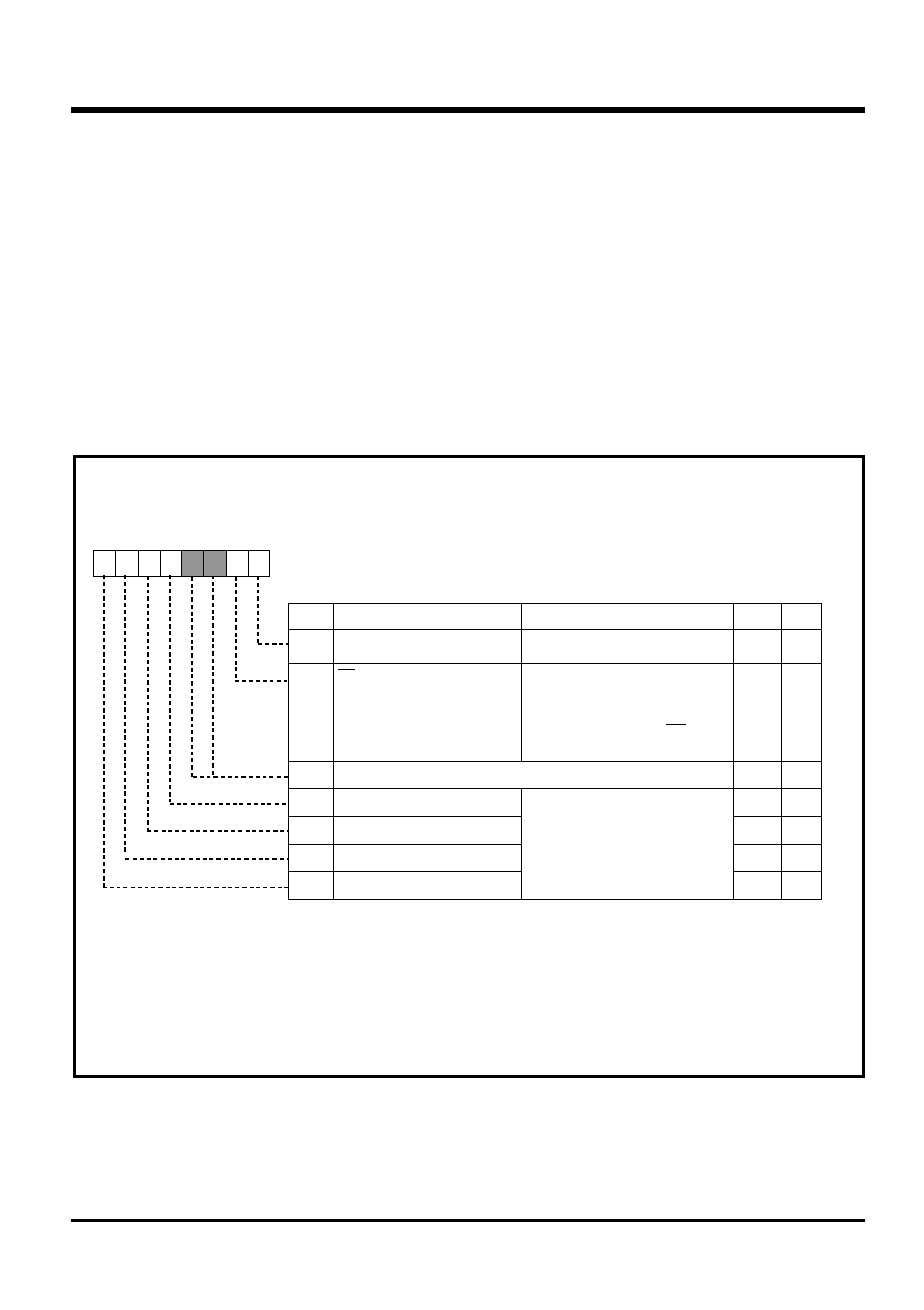
Fig. 13.2.4 Structure of DMAC control register L
13.2 Block description
13.2.2 DMAC control register L
Figure 13.2.4 shows the structure of DMAC control register L. Bit 0 is described in section “13.3.3 Channel
priority levels,” and bits 4–7 are also in section “13.3.2 DMA requests.”
(1)
___
TC
pin validity bit (Bit 1)
___
When this bit is set to “1,” port P103 functions as the TC pin. The TC pin is of an N-channel open-
drain type and provides the following functions:
q Terminal count signal output
When the transfer of an entire batch of data is normally terminated, the pin outputs “L” for 1
cycle of
φ. (Refer to section “13.3.5 (1) Normal termination.”)
q Forced termination signal input
___
When the TC pin’s input level goes from “H” to “L” during DMA transfer, this DMA transfer is forced
into termination. (Refer to section “13.3.5 (2) Forced termination.”)
Notes 1: The state of bits 4 to 7 is not changed when writing “1” to these bits.
2: When writing to this register while any of DMAi enable bits (bits 4 to 7 at address
6916) is “1,” use the LDM or STA instruction in m flag = “1.” When DMAi request bit
(bits 4 to 7 at address 6816) must not be changed, set DMAi request bit to “1.”
When writing to this register while all of DMAi enable bits (bits 4 to 7 at address 6916)
are “0,” m flag may be “0” or “1.” Use the LDM or STA instruction for writing to this
register. When DMAi request bit (bits 4 to 7 at address 6816) must not be changed,
set DMAi request bit to “1.”
0 : Fixed
1 : Rotating
Bit
Bit name
Functions
At reset
RW
0
1
Priority select bit
Undefined
0
0 : No request
1 : Requested (Note 1)
0
DMAC control register L (Address 6816)
b1
b0
b2
b3
b4
b5
b6
b7
RW
3, 2
0
RW
0
RW
TC pin validity bit
0 : Invalid
(P103 pin functions as a
programmable I/O port (CMOS).)
1 : Valid
(P103 pin functions as TC pin (N-
channel open-drain).)
Nothing is assigned.
–
4
5
6
7
DMA0 request bit
DMA1 request bit
DMA2 request bit
DMA3 request bit
0RW
0
RW
相關(guān)PDF資料 |
PDF描述 |
|---|---|
| M37733EHBFS | 16-BIT, UVPROM, 25 MHz, MICROCONTROLLER, CQCC80 |
| M37733EHLXXXHP | 16-BIT, OTPROM, 12 MHz, MICROCONTROLLER, PQFP80 |
| M37733MHBXXXFP | 16-BIT, MROM, 25 MHz, MICROCONTROLLER, PQFP80 |
| M37733S4LHP | 16-BIT, 12 MHz, MICROCONTROLLER, PQFP80 |
| M37734M8LXXXHP | 16-BIT, MROM, 12 MHz, MICROCONTROLLER, PQFP80 |
相關(guān)代理商/技術(shù)參數(shù) |
參數(shù)描述 |
|---|---|
| M37730026 | 制造商:Molex 功能描述: |
| M37733 | 制造商:MITSUBISHI 制造商全稱:Mitsubishi Electric Semiconductor 功能描述:16-BIT CMOS MICROCOMPUTER |
| M37733EHB | 制造商:MITSUBISHI 制造商全稱:Mitsubishi Electric Semiconductor 功能描述:PROM VERSION OF M37733MHBXXXFP(MICROCOMPUTERS) |
| M37733EHBFS | 制造商:RENESAS 制造商全稱:Renesas Technology Corp 功能描述:PROM VERSION OF M37733MHBXXXFP |
| M37733EHBXXXFP | 制造商:MITSUBISHI 制造商全稱:Mitsubishi Electric Semiconductor 功能描述:PROM VERSION OF M37733MHBXXXFP(MICROCOMPUTERS) |
發(fā)布緊急采購,3分鐘左右您將得到回復(fù)。