- 您現(xiàn)在的位置:買賣IC網(wǎng) > PDF目錄45028 > M3455AGC-XXXFP 4-BIT, OTPROM, 6 MHz, MICROCONTROLLER, PQFP52 PDF資料下載
參數(shù)資料
| 型號: | M3455AGC-XXXFP |
| 元件分類: | 微控制器/微處理器 |
| 英文描述: | 4-BIT, OTPROM, 6 MHz, MICROCONTROLLER, PQFP52 |
| 封裝: | 10 X 10 MM, 0.65 MM PITCH, PLASTIC, LQFP-52 |
| 文件頁數(shù): | 123/148頁 |
| 文件大小: | 1807K |
| 代理商: | M3455AGC-XXXFP |
第1頁第2頁第3頁第4頁第5頁第6頁第7頁第8頁第9頁第10頁第11頁第12頁第13頁第14頁第15頁第16頁第17頁第18頁第19頁第20頁第21頁第22頁第23頁第24頁第25頁第26頁第27頁第28頁第29頁第30頁第31頁第32頁第33頁第34頁第35頁第36頁第37頁第38頁第39頁第40頁第41頁第42頁第43頁第44頁第45頁第46頁第47頁第48頁第49頁第50頁第51頁第52頁第53頁第54頁第55頁第56頁第57頁第58頁第59頁第60頁第61頁第62頁第63頁第64頁第65頁第66頁第67頁第68頁第69頁第70頁第71頁第72頁第73頁第74頁第75頁第76頁第77頁第78頁第79頁第80頁第81頁第82頁第83頁第84頁第85頁第86頁第87頁第88頁第89頁第90頁第91頁第92頁第93頁第94頁第95頁第96頁第97頁第98頁第99頁第100頁第101頁第102頁第103頁第104頁第105頁第106頁第107頁第108頁第109頁第110頁第111頁第112頁第113頁第114頁第115頁第116頁第117頁第118頁第119頁第120頁第121頁第122頁當前第123頁第124頁第125頁第126頁第127頁第128頁第129頁第130頁第131頁第132頁第133頁第134頁第135頁第136頁第137頁第138頁第139頁第140頁第141頁第142頁第143頁第144頁第145頁第146頁第147頁第148頁
Rev.1.02
Nov 26, 2008
Page 76 of 146
REJ03B0224-0102
455A Group
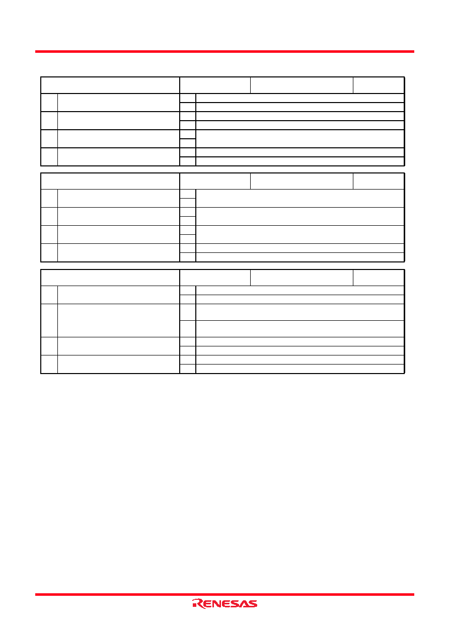
CONTROL REGISTERS
Note 1. “R” represents read enabled, and “W” represents write enabled.
Note 2. When the contents of I12 and I13 are changed, the external interrupt request flag (EXF0) may be set.
Interrupt control register V1
at reset : 00002
at power down : 00002
R/W (Note 1)
TAV1/TV1A
V13
Timer 2 interrupt enable bit
0
Interrupt disabled (SNZT2 instruction is valid)
1
Interrupt enabled (SNZT2 instruction is invalid)
V12
Timer 1 interrupt enable bit
0
Interrupt disabled (SNZT1 instruction is valid)
1
Interrupt enabled (SNZT1 instruction is invalid)
V11
Not used
0
This bit has no function, but read/write is enabled.
1
V10
External 0 interrupt enable bit
0
Interrupt disabled (SNZ0 instruction is valid)
1
Interrupt enabled (SNZ0 instruction is invalid)
Interrupt control register V2
at reset : 00002
at power down : 00002
R/W
TAV2/TV2A
V23
Not used
0
This bit has no function, but read/write is enabled.
1
V22
Not used
0
This bit has no function, but read/write is enabled.
1
V21
Not used
0
This bit has no function, but read/write is enabled.
1
V20
Timer 3 interrupt enable bit
0
Interrupt disabled (SNZT3 instruction is valid)
1
Interrupt enabled (SNZT3 instruction is invalid)
Interrupt control register I1
at reset : 00002
at power down : state retained
R/W
TAI1/TI1A
I13
INT pin input control bit (Note 2)
0
INT pin input disabled
1
INT pin input enabled
I12
Interrupt valid waveform for INT pin/
return level selection bit (Note 2)
0
Falling waveform (“L” level of INT pin is recognized with the SNZI0
instruction)/“L” level
1
Rising waveform (“H” level of INT pin is recognized with the SNZI0
instruction)/“H” level
I11
INT pin edge detection circuit control bit
0
One-sided edge detected
1
Both edges detected
I10
INT pin timer 1 count start synchronous
circuit selection bit
0
Timer 1 count start synchronous circuit not selected
1
Timer 1 count start synchronous circuit selected
相關(guān)PDF資料 |
PDF描述 |
|---|---|
| M3455AG8FP | 4-BIT, OTPROM, 6 MHz, MICROCONTROLLER, PQFP52 |
| M3455AGC-XXXFP | 4-BIT, OTPROM, 6 MHz, MICROCONTROLLER, PQFP52 |
| M3455AG8-XXXFP | 4-BIT, OTPROM, 6 MHz, MICROCONTROLLER, PQFP52 |
| M34570MD-XXXFP | 4-BIT, MROM, 2 MHz, MICROCONTROLLER, PDSO36 |
| M34570E8FP | 4-BIT, OTPROM, 2 MHz, MICROCONTROLLER, PDSO36 |
相關(guān)代理商/技術(shù)參數(shù) |
參數(shù)描述 |
|---|---|
| M3455-SL001 | 制造商:Alpha Wire 功能描述: |
| M3455-SL002 | 制造商:Alpha Wire 功能描述: |
| M3455-SL005 | 制造商:Alpha Wire 功能描述: |
| M3455-SL199 | 制造商:Alpha Wire 功能描述: |
| M3455-SLATE-100 | 制造商:Alpha Wire 功能描述: |
發(fā)布緊急采購,3分鐘左右您將得到回復。