- 您現(xiàn)在的位置:買賣IC網(wǎng) > PDF目錄44992 > LTC3707IGN-SYNC (LINEAR TECHNOLOGY CORP) 3 A SWITCHING CONTROLLER, 360 kHz SWITCHING FREQ-MAX, PDSO28 PDF資料下載
參數(shù)資料
| 型號: | LTC3707IGN-SYNC |
| 廠商: | LINEAR TECHNOLOGY CORP |
| 元件分類: | 穩(wěn)壓器 |
| 英文描述: | 3 A SWITCHING CONTROLLER, 360 kHz SWITCHING FREQ-MAX, PDSO28 |
| 封裝: | 0.150 INCH, PLASTIC, SSOP-28 |
| 文件頁數(shù): | 15/32頁 |
| 文件大?。?/td> | 403K |
| 代理商: | LTC3707IGN-SYNC |
第1頁第2頁第3頁第4頁第5頁第6頁第7頁第8頁第9頁第10頁第11頁第12頁第13頁第14頁當前第15頁第16頁第17頁第18頁第19頁第20頁第21頁第22頁第23頁第24頁第25頁第26頁第27頁第28頁第29頁第30頁第31頁第32頁
LTC3707-SYNC
22
3707sfa
The secondary output voltage VSECisnormallysetasshown
in Figure 6a by the turns ratio N of the transformer:
VSEC (N + 1) VOUT
However, if the controller goes into Burst Mode operation
and halts switching due to a light primary load current, then
VSEC will droop. An external resistive divider from VSEC to
the FCB pin sets a minimum voltage VSEC(MIN):
VV
R
SEC MIN
()
.
≈+
08
1
6
5
where R5 and R6 are shown in Figure 2.
If VSEC drops below this level, the FCB voltage forces
temporary continuous switching operation until VSEC is
again above its minimum.
In order to prevent erratic operation if no external connec-
tions are made to the FCB pin, the FCB pin has a 0.18μA
internal current source pulling the pin high. Include this
current when choosing resistor values R5 and R6.
The following table summarizes the possible states
available on the FCB pin:
Table 1
FCB PIN
CONDITION
0V to 0.75V
Forced Continuous Both Controllers
(Current Reversal Allowed—
Burst Inhibited)
0.85V < VFCB < 4.3V
Minimum Peak Current Induces
Burst Mode Operation
No Current Reversal Allowed
Feedback Resistors
Regulating a Secondary Winding
>4.8V
Burst Mode Operation Disabled
Constant Frequency Mode Enabled
No Current Reversal Allowed
No Minimum Peak Current
Voltage Positioning
Voltage positioning can be used to minimize peak-to-peak
output voltage excursions under worst-case transient
loading conditions. The open-loop DC gain of the control
loop is reduced depending upon the maximum load step
specications. Voltage positioning can easily be added to
the controller by loading the ITH pin with a resistive divider
having a Thevenin equivalent voltage source equal to the
APPLICATIONS INFORMATION
midpoint operating voltage range of the error amplier, or
1.2V (see Figure 8).
The resistive load reduces the DC loop gain while main-
taining the linear control range of the error amplier.
The maximum output voltage deviation can theoretically
be reduced to half or alternatively the amount of output
capacitance can be reduced for a particular application.
A complete explanation is included in Design Solutions
10. (See www.linear-tech.com)
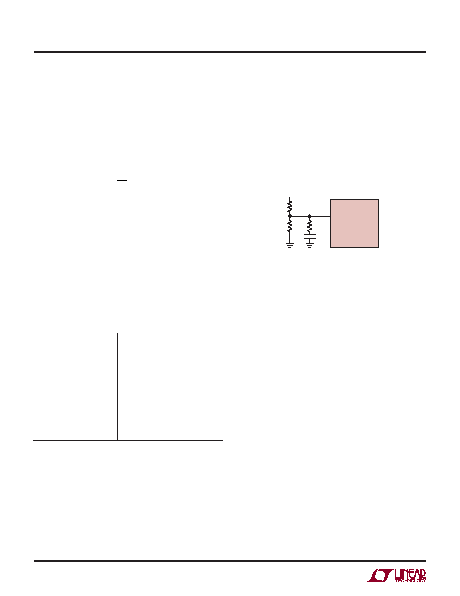
ITH
RC
RT1
INTVCC
CC
3707 F08
LTC3707-SYNC
RT2
Figure 8. Active Voltage Positioning Applied
to the LTC3707-SYNC
Efciency Considerations
The percent efciency of a switching regulator is equal to
the output power divided by the input power times 100%.
It is often useful to analyze individual losses to determine
what is limiting the efciency and which change would
produce the most improvement. Percent efciency can
be expressed as:
%Efciency = 100% – (L1 + L2 + L3 + ...)
where L1, L2, etc. are the individual losses as a percentage
of input power.
Although all dissipative elements in the circuit produce
losses, four main sources usually account for most of the
losses in application circuits: 1) IC VIN current (including
loading on the 3.3V internal regulator), 2) INTVCC regulator
current, 3) I2R losses, 4) Topside MOSFET transition
losses.
1. The VIN current has two components: the rst is the DC
supply current given in the Electrical Characteristics table,
which excludes MOSFET driver and control currents; the
second is the current drawn from the 3.3V linear regulator
output. VIN current typically results in a small (<0.1%)
loss.
相關(guān)PDF資料 |
PDF描述 |
|---|---|
| LTC3728IUH | 3 A DUAL SWITCHING CONTROLLER, 590 kHz SWITCHING FREQ-MAX, PQCC32 |
| LTC3728IG | 3 A DUAL SWITCHING CONTROLLER, 590 kHz SWITCHING FREQ-MAX, PDSO28 |
| LTC3728LIUH-1#TR | 3 A DUAL SWITCHING CONTROLLER, 590 kHz SWITCHING FREQ-MAX, PQCC32 |
| LTC3728LIGN-1 | 3 A DUAL SWITCHING CONTROLLER, 590 kHz SWITCHING FREQ-MAX, PDSO28 |
| LTC3731HUH#TRPBF | 5 A SWITCHING CONTROLLER, 750 kHz SWITCHING FREQ-MAX, PQCC32 |
相關(guān)代理商/技術(shù)參數(shù) |
參數(shù)描述 |
|---|---|
| LTC3707IGN-SYNC#PBF | 功能描述:IC REG CTRLR BUCK PWM CM 28-SSOP RoHS:是 類別:集成電路 (IC) >> PMIC - 穩(wěn)壓器 - DC DC 切換控制器 系列:PolyPhase® 標準包裝:4,500 系列:PowerWise® PWM 型:控制器 輸出數(shù):1 頻率 - 最大:1MHz 占空比:95% 電源電壓:2.8 V ~ 5.5 V 降壓:是 升壓:無 回掃:無 反相:無 倍增器:無 除法器:無 Cuk:無 隔離:無 工作溫度:-40°C ~ 125°C 封裝/外殼:6-WDFN 裸露焊盤 包裝:帶卷 (TR) 配用:LM1771EVAL-ND - BOARD EVALUATION LM1771 其它名稱:LM1771SSDX |
| LTC3707IGN-SYNC#TRPBF | 功能描述:IC REG CTRLR BUCK PWM CM 28-SSOP RoHS:是 類別:集成電路 (IC) >> PMIC - 穩(wěn)壓器 - DC DC 切換控制器 系列:PolyPhase® 標準包裝:4,500 系列:PowerWise® PWM 型:控制器 輸出數(shù):1 頻率 - 最大:1MHz 占空比:95% 電源電壓:2.8 V ~ 5.5 V 降壓:是 升壓:無 回掃:無 反相:無 倍增器:無 除法器:無 Cuk:無 隔離:無 工作溫度:-40°C ~ 125°C 封裝/外殼:6-WDFN 裸露焊盤 包裝:帶卷 (TR) 配用:LM1771EVAL-ND - BOARD EVALUATION LM1771 其它名稱:LM1771SSDX |
| LTC3708EUH | 功能描述:IC REG CTRLR BUCK PWM CM 32-QFN RoHS:否 類別:集成電路 (IC) >> PMIC - 穩(wěn)壓器 - DC DC 切換控制器 系列:PolyPhase® 標準包裝:4,500 系列:PowerWise® PWM 型:控制器 輸出數(shù):1 頻率 - 最大:1MHz 占空比:95% 電源電壓:2.8 V ~ 5.5 V 降壓:是 升壓:無 回掃:無 反相:無 倍增器:無 除法器:無 Cuk:無 隔離:無 工作溫度:-40°C ~ 125°C 封裝/外殼:6-WDFN 裸露焊盤 包裝:帶卷 (TR) 配用:LM1771EVAL-ND - BOARD EVALUATION LM1771 其它名稱:LM1771SSDX |
| LTC3708EUH#PBF | 功能描述:IC REG CTRLR BUCK PWM CM 32-QFN RoHS:是 類別:集成電路 (IC) >> PMIC - 穩(wěn)壓器 - DC DC 切換控制器 系列:PolyPhase® 特色產(chǎn)品:LM3753/54 Scalable 2-Phase Synchronous Buck Controllers 標準包裝:1 系列:PowerWise® PWM 型:電壓模式 輸出數(shù):1 頻率 - 最大:1MHz 占空比:81% 電源電壓:4.5 V ~ 18 V 降壓:是 升壓:無 回掃:無 反相:無 倍增器:無 除法器:無 Cuk:無 隔離:無 工作溫度:-5°C ~ 125°C 封裝/外殼:32-WFQFN 裸露焊盤 包裝:Digi-Reel® 產(chǎn)品目錄頁面:1303 (CN2011-ZH PDF) 其它名稱:LM3754SQDKR |
| LTC3708EUH#TR | 功能描述:IC REG CTRLR BUCK PWM CM 32-QFN RoHS:否 類別:集成電路 (IC) >> PMIC - 穩(wěn)壓器 - DC DC 切換控制器 系列:PolyPhase® 標準包裝:4,500 系列:PowerWise® PWM 型:控制器 輸出數(shù):1 頻率 - 最大:1MHz 占空比:95% 電源電壓:2.8 V ~ 5.5 V 降壓:是 升壓:無 回掃:無 反相:無 倍增器:無 除法器:無 Cuk:無 隔離:無 工作溫度:-40°C ~ 125°C 封裝/外殼:6-WDFN 裸露焊盤 包裝:帶卷 (TR) 配用:LM1771EVAL-ND - BOARD EVALUATION LM1771 其它名稱:LM1771SSDX |
發(fā)布緊急采購,3分鐘左右您將得到回復。