- 您現(xiàn)在的位置:買賣IC網(wǎng) > PDF目錄358934 > LPC47M172 (SMSC Corporation) ADVANCED I/O CONTROLLER WITH MOTHERBOARD GLUE LOGIC PDF資料下載
參數(shù)資料
| 型號(hào): | LPC47M172 |
| 廠商: | SMSC Corporation |
| 英文描述: | ADVANCED I/O CONTROLLER WITH MOTHERBOARD GLUE LOGIC |
| 中文描述: | 先進(jìn)的I / O控制器與主板膠合邏輯 |
| 文件頁(yè)數(shù): | 65/228頁(yè) |
| 文件大小: | 1269K |
| 代理商: | LPC47M172 |
第1頁(yè)第2頁(yè)第3頁(yè)第4頁(yè)第5頁(yè)第6頁(yè)第7頁(yè)第8頁(yè)第9頁(yè)第10頁(yè)第11頁(yè)第12頁(yè)第13頁(yè)第14頁(yè)第15頁(yè)第16頁(yè)第17頁(yè)第18頁(yè)第19頁(yè)第20頁(yè)第21頁(yè)第22頁(yè)第23頁(yè)第24頁(yè)第25頁(yè)第26頁(yè)第27頁(yè)第28頁(yè)第29頁(yè)第30頁(yè)第31頁(yè)第32頁(yè)第33頁(yè)第34頁(yè)第35頁(yè)第36頁(yè)第37頁(yè)第38頁(yè)第39頁(yè)第40頁(yè)第41頁(yè)第42頁(yè)第43頁(yè)第44頁(yè)第45頁(yè)第46頁(yè)第47頁(yè)第48頁(yè)第49頁(yè)第50頁(yè)第51頁(yè)第52頁(yè)第53頁(yè)第54頁(yè)第55頁(yè)第56頁(yè)第57頁(yè)第58頁(yè)第59頁(yè)第60頁(yè)第61頁(yè)第62頁(yè)第63頁(yè)第64頁(yè)當(dāng)前第65頁(yè)第66頁(yè)第67頁(yè)第68頁(yè)第69頁(yè)第70頁(yè)第71頁(yè)第72頁(yè)第73頁(yè)第74頁(yè)第75頁(yè)第76頁(yè)第77頁(yè)第78頁(yè)第79頁(yè)第80頁(yè)第81頁(yè)第82頁(yè)第83頁(yè)第84頁(yè)第85頁(yè)第86頁(yè)第87頁(yè)第88頁(yè)第89頁(yè)第90頁(yè)第91頁(yè)第92頁(yè)第93頁(yè)第94頁(yè)第95頁(yè)第96頁(yè)第97頁(yè)第98頁(yè)第99頁(yè)第100頁(yè)第101頁(yè)第102頁(yè)第103頁(yè)第104頁(yè)第105頁(yè)第106頁(yè)第107頁(yè)第108頁(yè)第109頁(yè)第110頁(yè)第111頁(yè)第112頁(yè)第113頁(yè)第114頁(yè)第115頁(yè)第116頁(yè)第117頁(yè)第118頁(yè)第119頁(yè)第120頁(yè)第121頁(yè)第122頁(yè)第123頁(yè)第124頁(yè)第125頁(yè)第126頁(yè)第127頁(yè)第128頁(yè)第129頁(yè)第130頁(yè)第131頁(yè)第132頁(yè)第133頁(yè)第134頁(yè)第135頁(yè)第136頁(yè)第137頁(yè)第138頁(yè)第139頁(yè)第140頁(yè)第141頁(yè)第142頁(yè)第143頁(yè)第144頁(yè)第145頁(yè)第146頁(yè)第147頁(yè)第148頁(yè)第149頁(yè)第150頁(yè)第151頁(yè)第152頁(yè)第153頁(yè)第154頁(yè)第155頁(yè)第156頁(yè)第157頁(yè)第158頁(yè)第159頁(yè)第160頁(yè)第161頁(yè)第162頁(yè)第163頁(yè)第164頁(yè)第165頁(yè)第166頁(yè)第167頁(yè)第168頁(yè)第169頁(yè)第170頁(yè)第171頁(yè)第172頁(yè)第173頁(yè)第174頁(yè)第175頁(yè)第176頁(yè)第177頁(yè)第178頁(yè)第179頁(yè)第180頁(yè)第181頁(yè)第182頁(yè)第183頁(yè)第184頁(yè)第185頁(yè)第186頁(yè)第187頁(yè)第188頁(yè)第189頁(yè)第190頁(yè)第191頁(yè)第192頁(yè)第193頁(yè)第194頁(yè)第195頁(yè)第196頁(yè)第197頁(yè)第198頁(yè)第199頁(yè)第200頁(yè)第201頁(yè)第202頁(yè)第203頁(yè)第204頁(yè)第205頁(yè)第206頁(yè)第207頁(yè)第208頁(yè)第209頁(yè)第210頁(yè)第211頁(yè)第212頁(yè)第213頁(yè)第214頁(yè)第215頁(yè)第216頁(yè)第217頁(yè)第218頁(yè)第219頁(yè)第220頁(yè)第221頁(yè)第222頁(yè)第223頁(yè)第224頁(yè)第225頁(yè)第226頁(yè)第227頁(yè)第228頁(yè)
Note
: The UARTs 1 and 2 may be configured to share an interrupt. Refer to the Configuration section for more
information.
SMSC DS – LPC47M192
Page 65
Rev. 03/30/05
DATASHEET
REGISTER DESCRIPTION
Addressing of the accessible registers of the Serial Port is shown below. The base addresses of the serial ports are
defined by the configuration registers (see “Configuration” section). The Serial Port registers are located at
sequentially increasing addresses above these base addresses. The LPC47M192 contains two serial ports, each of
which contain a register set as described below.
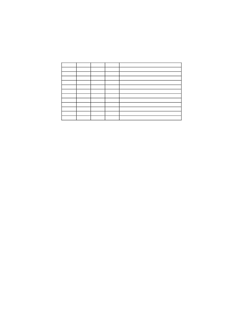
Table 28 – Addressing the Serial Port
DLAB*
0
0
0
X
X
X
X
X
X
X
1
1
A2
0
0
0
0
0
0
1
1
1
1
0
0
A1
0
0
0
1
1
1
0
0
1
1
0
0
A0
0
0
1
0
0
1
0
1
0
1
0
1
REGISTER NAME
Receive Buffer (read)
Transmit Buffer (write)
Interrupt Enable (read/write)
Interrupt Identification (read)
FIFO Control (write)
Line Control (read/write)
Modem Control (read/write)
Line Status (read/write)
Modem Status (read/write)
Scratchpad (read/write)
Divisor LSB (read/write)
Divisor MSB (read/write
*Note
: DLAB is Bit 7 of the Line Control Register
The following section describes the operation of the registers.
RECEIVE BUFFER REGISTER (RB)
Address Offset = 0H, DLAB = 0, READ ONLY
This register holds the received incoming data byte. Bit 0 is the least significant bit, which is transmitted and received
first. Received data is double buffered; this uses an additional shift register to receive the serial data stream and
convert it to a parallel 8 bit word which is transferred to the Receive Buffer register. The shift register is not
accessible.
TRANSMIT BUFFER REGISTER (TB)
Address Offset = 0H, DLAB = 0, WRITE ONLY
This register contains the data byte to be transmitted. The transmit buffer is double buffered, utilizing an additional
shift register (not accessible) to convert the 8 bit data word to a serial format. This shift register is loaded from the
Transmit Buffer when the transmission of the previous byte is complete.
INTERRUPT ENABLE REGISTER (IER)
Address Offset = 1H, DLAB = 0, READ/WRITE
The lower four bits of this register control the enables of the five interrupt sources of the Serial Port interrupt. It is
possible to totally disable the interrupt system by resetting bits 0 through 3 of this register. Similarly, setting the
appropriate bits of this register to a high, selected interrupts can be enabled. Disabling the interrupt system inhibits
the Interrupt Identification Register and disables any Serial Port interrupt out of the LPC47M192. All other system
functions operate in their normal manner, including the Line Status and MODEM Status Registers. The contents of
the Interrupt Enable Register are described below.
Bit 0
This bit enables the Received Data Available Interrupt (and timeout interrupts in the FIFO mode) when set to logic
“1”.
相關(guān)PDF資料 |
PDF描述 |
|---|---|
| LPC47N252 | Advanced Notebook I/O Controller with On-Board FLASH |
| LPC47N267 | 100 Pin LPC Notebook I/O with X-Bus Interface |
| LPC47M112 | ENHANCED SUPER I/O CONTROLLER WITH LPC INTERFACE |
| LPC47M112-MC | ENHANCED SUPER I/O CONTROLLER WITH LPC INTERFACE |
| LPC47M112-MW | ENHANCED SUPER I/O CONTROLLER WITH LPC INTERFACE |
相關(guān)代理商/技術(shù)參數(shù) |
參數(shù)描述 |
|---|---|
| LPC47M172_07 | 制造商:SMSC 制造商全稱:SMSC 功能描述:Advanced I/O Controller with Motherboard GLUE Logic |
| LPC47M172-NR | 制造商:SMSC 功能描述:MULTIFUNCTION PERIPHERAL, PQFP128 |
| LPC47M172-NW | 功能描述:輸入/輸出控制器接口集成電路 Enhanced Super I/O Contrllr RoHS:否 制造商:Silicon Labs 產(chǎn)品: 輸入/輸出端數(shù)量: 工作電源電壓: 最大工作溫度:+ 85 C 最小工作溫度:- 40 C 安裝風(fēng)格:SMD/SMT 封裝 / 箱體:QFN-64 封裝:Tray |
| LPC47M182 | 制造商:SMSC 制造商全稱:SMSC 功能描述:ADVANCED I/O CONTROLLER WITH MOTHERBOARD GLUE LOGIC |
| LPC47M182_07 | 制造商:SMSC 制造商全稱:SMSC 功能描述:Advanced I/O Controller with Motherboard GLUE Logic |
發(fā)布緊急采購(gòu),3分鐘左右您將得到回復(fù)。