- 您現(xiàn)在的位置:買賣IC網(wǎng) > PDF目錄358934 > LPC47M112-MW (STANDARD MICROSYSTEMS CORP) ENHANCED SUPER I/O CONTROLLER WITH LPC INTERFACE PDF資料下載
參數(shù)資料
| 型號: | LPC47M112-MW |
| 廠商: | STANDARD MICROSYSTEMS CORP |
| 元件分類: | 外設及接口 |
| 英文描述: | ENHANCED SUPER I/O CONTROLLER WITH LPC INTERFACE |
| 中文描述: | MULTIFUNCTION PERIPHERAL, PQFP100 |
| 封裝: | 14 X 20 MM, ROHS COMPLIANT, QFP-100 |
| 文件頁數(shù): | 19/228頁 |
| 文件大?。?/td> | 1269K |
| 代理商: | LPC47M112-MW |
第1頁第2頁第3頁第4頁第5頁第6頁第7頁第8頁第9頁第10頁第11頁第12頁第13頁第14頁第15頁第16頁第17頁第18頁當前第19頁第20頁第21頁第22頁第23頁第24頁第25頁第26頁第27頁第28頁第29頁第30頁第31頁第32頁第33頁第34頁第35頁第36頁第37頁第38頁第39頁第40頁第41頁第42頁第43頁第44頁第45頁第46頁第47頁第48頁第49頁第50頁第51頁第52頁第53頁第54頁第55頁第56頁第57頁第58頁第59頁第60頁第61頁第62頁第63頁第64頁第65頁第66頁第67頁第68頁第69頁第70頁第71頁第72頁第73頁第74頁第75頁第76頁第77頁第78頁第79頁第80頁第81頁第82頁第83頁第84頁第85頁第86頁第87頁第88頁第89頁第90頁第91頁第92頁第93頁第94頁第95頁第96頁第97頁第98頁第99頁第100頁第101頁第102頁第103頁第104頁第105頁第106頁第107頁第108頁第109頁第110頁第111頁第112頁第113頁第114頁第115頁第116頁第117頁第118頁第119頁第120頁第121頁第122頁第123頁第124頁第125頁第126頁第127頁第128頁第129頁第130頁第131頁第132頁第133頁第134頁第135頁第136頁第137頁第138頁第139頁第140頁第141頁第142頁第143頁第144頁第145頁第146頁第147頁第148頁第149頁第150頁第151頁第152頁第153頁第154頁第155頁第156頁第157頁第158頁第159頁第160頁第161頁第162頁第163頁第164頁第165頁第166頁第167頁第168頁第169頁第170頁第171頁第172頁第173頁第174頁第175頁第176頁第177頁第178頁第179頁第180頁第181頁第182頁第183頁第184頁第185頁第186頁第187頁第188頁第189頁第190頁第191頁第192頁第193頁第194頁第195頁第196頁第197頁第198頁第199頁第200頁第201頁第202頁第203頁第204頁第205頁第206頁第207頁第208頁第209頁第210頁第211頁第212頁第213頁第214頁第215頁第216頁第217頁第218頁第219頁第220頁第221頁第222頁第223頁第224頁第225頁第226頁第227頁第228頁
SMSC DS – LPC47M192
Page 19
Rev. 03/30/05
DATASHEET
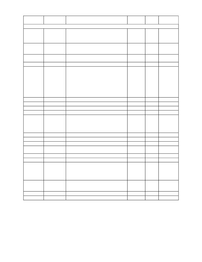
QFP PIN#
NAME
DESCRIPTION
BUFFER
NAME
PWR
WELL
NOTES
HARDWARE MONITORING BLOCK (28)
+3.3V VCC pin dedicated to the Hardware
Monitoring block. Can be powered by
+3.3V Standby power if monitoring in low
power states is required.
Analog Ground. Internally connected to all
of the Hardware Monitoring Block circuitry.
102, 111,
121, 122
HVCC
1
101, 112,
125, 126,
127, 128
103
HVSS
1
SDA
System Management Bus bi-directional
Data. Open Drain output.
System Management Bus Clock.
The lowest order programmable bit of the
SMBus Address Input.
Minimum 20msec low Reset output pulse
Interrupt output for temperature and voltage
interrupts.
XNOR-Chain test mode Output
The RESET# and THERM# are Open-Drain
Outputs
Voltage ID 0 Input
Voltage ID 1 Input
Voltage ID 2 Input
Voltage ID 3 Input
Defaults to Analog Input for +12V.
Optionally, can be configured to read the
VID4 Digital Input, a voltage supply readout
from the processor. This value is read in the
VID4 Register.
Analog input for +5V
Analog input for +3.3V
Analog input for +2.5V
Analog input for +Vccp (processor voltage:
0 to 3.0V).
Analog input for +1.8V
Analog Input for +1.5V
This is the negative Analog input (current
sink) from the remote thermal diode. This
serves as the negative input into the A/D.
Digital Input. If held high at power-up,
initiates XNOR chain test mode.
This is the positive input (current source)
from the remote thermal diode. This serves
as the positive input into the A/D.
See D0+ description.
See D0- negative analog input description.
I
M
OD3
HVCC
104
105
SCLK
A0/
RESET#/
THERM#/
XNOR_OUT
I
M
I
M
O3
HVCC
HVCC
106
107
108
109
110
VID0
VID1
VID2
VID3
12V_IN/
VID4
I
M
I
M
I
M
I
M
I
ANG
/I
M
HVCC
HVCC
HVCC
HVCC
HVCC
115
116
117
118
+5V_IN
+3.3V_IN
+2.5V_IN
Vccp_IN
I
ANG
I
ANG
I
ANG
I
ANG
119
120
113
+1.8V_IN
+1.5V_IN
D0-/
XNOR_IN
I
ANG
I
ANG
I
ANG
/I
M
HVCC
114
D0+
I
ANG
HVCC
123
124
D1+
D1-
I
ANG
I
ANG
HVCC
HVCC
Note
:
The “n” as the first letter of a signal name or the “#” as the suffix of a signal name indicates an “Active Low”
signal.
Note 1
: VCC and VSS pins are for Super I/O Blocks. HVCC and HVSS are dedicated for the Hardware Monitoring
Block.
Note 2
:
VTR can be connected to VCC if no wakeup functionality is required.
Note 3
:
If the 32kHz input clock is not used the CLKI32 pin must be grounded. There is a bit in the configuration
register at 0xF0 in Logical Device A that indicates whether or not the 32KHz clock is connected. This bit
determines the clock source for the fan tachometer, LED and “wake on specific key” logic. Set this bit to ‘1’
if the clock is not connected.
相關PDF資料 |
PDF描述 |
|---|---|
| LPC47N252-SD | Advanced Notebook I/O Controller with On-Board FLASH |
| LPC47N252-SG | Advanced Notebook I/O Controller with On-Board FLASH |
| LPC47M172-NR | ADVANCED I/O CONTROLLER WITH MOTHERBOARD GLUE LOGIC |
| LPC47N267-MN | 100 Pin LPC Notebook I/O with X-Bus Interface |
| LPC47N227-MN | 100 Pin Super I/O with LPC Interface for Notebook Applications |
相關代理商/技術參數(shù) |
參數(shù)描述 |
|---|---|
| LPC47M133-NC | 制造商:SMSC 功能描述: |
| LPC47M140-NC | 制造商:SMSC 制造商全稱:SMSC 功能描述:128 PIN ENGANCED SUPER I/O CONTROLLER WITH AN LPC INTERFACE AND USB HUB |
| LPC47M141-NC | 制造商:SMSC 制造商全稱:SMSC 功能描述:128 PIN ENGANCED SUPER I/O CONTROLLER WITH AN LPC INTERFACE AND USB HUB |
| LPC47M142-NC | 制造商:Rochester Electronics LLC 功能描述:- Bulk |
| LPC47M143-NC | 制造商:Rochester Electronics LLC 功能描述:- Bulk |
發(fā)布緊急采購,3分鐘左右您將得到回復。