- 您現(xiàn)在的位置:買賣IC網(wǎng) > PDF目錄384605 > LMX9838SBX (NATIONAL SEMICONDUCTOR CORP) Bluetooth Serial Port Module PDF資料下載
參數(shù)資料
| 型號: | LMX9838SBX |
| 廠商: | NATIONAL SEMICONDUCTOR CORP |
| 元件分類: | 通信及網(wǎng)絡(luò) |
| 英文描述: | Bluetooth Serial Port Module |
| 中文描述: | SPECIALTY TELECOM CIRCUIT, PBGA70 |
| 封裝: | 10 X 17 MM, 2 MM HEIGHT, LGA-70 |
| 文件頁數(shù): | 11/26頁 |
| 文件大小: | 974K |
| 代理商: | LMX9838SBX |
第1頁第2頁第3頁第4頁第5頁第6頁第7頁第8頁第9頁第10頁當(dāng)前第11頁第12頁第13頁第14頁第15頁第16頁第17頁第18頁第19頁第20頁第21頁第22頁第23頁第24頁第25頁第26頁
12.3 RECEIVER BACK-END
The hard-limiters are followed by a two frequency discrimina-
tors. The I-frequency discriminator uses the 90× phase-shift-
ed signal from the Q-path, while the Q-discriminator uses the
90× phase-shifted signal from the I-path. A poly-phase band-
pass filter performs the required phase shifting. The output
signals of the I- and Q-discriminator are substracted and fil-
tered by a low-pass filter. An equalizer is added to improve
the eye-pattern for 101010 patterns.
After equalization, a dynamic AFC (automatic frequency off-
set compensation) circuit and slicer extract the RX_DATA
from the analog data pattern. It is expected that the Eb/No of
the demodulator is approximately 17 dB.
12.3.1 Frequency Discriminator
The frequency discriminator gets its input signals from the
limiter. A defined signal level (independent of the power sup-
ply voltage) is needed to obtain the input signal. Both inputs
of the frequency discriminator have limiting circuits to opti-
mize performance. The bandpass filter in the frequency dis-
criminator is tuned by the autotuning circuitry.
12.3.2 Post-Detection Filter and Equalizer
The output signals of the FM discriminator first go through a
post-detection filter and then through an equalizer. Both the
post-detection filter and equalizer are tuned to the proper fre-
quency by the autotuning circuitry. The post-detection filter is
a low-pass filter intended to suppress all remaining spurious
signals, such as the second harmonic (4 MHz) from the FM
detector and noise generated after the limiter.
The post-detection filter also helps for attenuating the first
adjacent channel signal. The equalizer improves the eye-
opening for 101010 patterns. The post-detection filter is a
third order Butterworth filter.
12.4 AUTOTUNING CIRCUITRY
The autotuning circuitry is used for tuning the bandpass filter,
the detector, the post-detection filter, the equalizer, and the
transmit filters for process and temperature variations. The
circuit also includes an offset compensation for the FM de-
tector.
12.5 SYNTHESIZER
The synthesizer consists of a phase-frequency detector, a
charge pump, a low-pass loop filter, a programmable fre-
quency divider, a voltage-controlled oscillator (VCO), a delta-
sigma modulator, and a lookup table.
The frequency divider consists of a divide-by-2 circuit (divides
the 5 GHz signal from the VCO down to 2.5 GHz), a divide-
by-8-or-9 divider, and a digital modulus control. The delta-
sigma modulator controls the division ratio and also gener-
ates an input channel value to the lookup table.
12.5.1 Phase-Frequency Detector
The phase-frequency detector is a 5-state phase-detector. It
responds only to transitions, hence phase-error is indepen-
dent of input waveform duty cycle or amplitude variations.
Loop lockup occurs when all the negative transitions on the
inputs, F_REF and F_MOD, coincide. Both outputs (i.e., Up
and Down) then remain high. This is equal to the zero error
mode. The phase-frequency detector input frequency range
operates at 12 MHz.
12.6 TRANSMITTER CIRCUITRY
The transmitter consists of ROM tables, two Digital to Analog
(DA) converters, two low-pass filters, IQ mixers, and a power
amplifier (PA).
The ROM tables generate a digital IQ signal based on the
transmit data. The output of the ROM tables is inserted into
IQ-DA converters and filtered through two low-pass filters.
The two signal components are mixed up to 2.5 GHz by the
TX mixers and added together before being inserted into the
transmit PA.
12.6.1 IQ-DA Converters and TX Mixers
The ROM output signals drive an I- and a Q-DA converter.
Two Butterworth low-pass filters filter the DA output signals.
The 6 MHz clock for the DA converters and the logic circuitry
around the ROM tables are derived from the autotuner.
The TX mixers mix the balanced I- and Q-signals up to 2.4-2.5
GHz. The output signals of the I- and Q-mixers are summed.
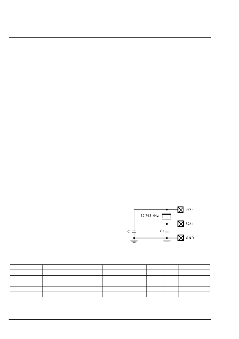
12.7 32 kHz Oscillator
An oscillator is provided (see
Figure 3
) that is tuned to provide
optimum performance and low-power consumption while op-
erating with a 32.768 kHz crystal. An external crystal clock
network is required between the 32k+ clock input (pad 27) and
the 32k- clock output (pad 28) signals.The oscillator is built in
a Pierce configuration and uses two external capacitors.
Ta-
ble 13
provides the oscillator’s specifications.
In case the 32kHz is not used, it is recommended to leave
32k- open and connect 32k+ to GND.
30027903
FIGURE 3. 32.768 kHz Oscillator
TABLE 13. 32.768 kHz Oscillator Specifications
Symbol
Parameter
Condition
Min
1.62
Typ
1.8
Max
1.98
Unit
V
V
DD
I
DDACT
f
V
PPOSC
Supply Voltage
Supply Current (Active)
2
μA
kHz
V
%
Nominal Output Frequency
Oscillating Amplitude
32.768
1.8
-
Duty Cycle
40
60
11
www.national.com
L
相關(guān)PDF資料 |
PDF描述 |
|---|---|
| LNBEH21 | LNB SUPPLY AND CONTROL IC WITH STEP-UP CONVERTER AND IC INTERFACE |
| LNBEH21PD | LNB SUPPLY AND CONTROL IC WITH STEP-UP CONVERTER AND IC INTERFACE |
| LNBEH21PD-TR | LNB SUPPLY AND CONTROL IC WITH STEP-UP CONVERTER AND IC INTERFACE |
| LNBK10 | LNB Supply And Control Voltage Regulator (Parallel Interface)(LNB 電源及控制電壓穩(wěn)壓器(并行接口)) |
| LP2950L-XX-T92-K | 100 mA LOW-DROPOUT VOLTAGE REGULATOR |
相關(guān)代理商/技術(shù)參數(shù) |
參數(shù)描述 |
|---|---|
| LMX9838SBX/NOPB | 功能描述:藍(lán)牙/802.15.1 模塊 RoHS:否 制造商:Murata Wireless Solutions 類:1 頻帶:2402 MHz to 2480 MHz 靈敏度:- 92 dBm 數(shù)據(jù)速率: 工作電源電壓:2.2 V to 3.3 V 輸出功率: 接口類型:PCM, UART 天線連接器類型:Chip 最大工作溫度:+ 85 C 尺寸:17.5 mm x 16 mm x 2 mm |
| LMXA301 | 制造商:Maglite 功能描述:3 Cell Lamp 制造商:MAG 功能描述:MAG 3 CELL LAMP, FOR USE WITH: MAG D CELL FLASHLIGHT 29-2000, MAG D CELL FLASHLIGHT 29-2010 制造商:Magnecraft 功能描述:MAGLITE LMXA301 LAMPS 3 CELL |
| LMXA301L | 制造商:MAG-LITE 功能描述: |
| LMXA401 | 制造商:Maglite 功能描述:4 Cell Lamp 制造商:MAG 功能描述:MAGLITE LMXA401 LAMPS 4 CELL 制造商:MAG 功能描述:MAG 4 CELL LAMP, FOR USE WITH: MAG D CELL FLASHLIGHT 29-2015, MAG D CELL FLASHLIGHT 29-2020 |
| LMXA401L | 制造商:MAG-LITE 功能描述: |
發(fā)布緊急采購,3分鐘左右您將得到回復(fù)。