- 您現(xiàn)在的位置:買賣IC網(wǎng) > PDF目錄384605 > LMX9838SBX (NATIONAL SEMICONDUCTOR CORP) Bluetooth Serial Port Module PDF資料下載
參數(shù)資料
| 型號(hào): | LMX9838SBX |
| 廠商: | NATIONAL SEMICONDUCTOR CORP |
| 元件分類: | 通信及網(wǎng)絡(luò) |
| 英文描述: | Bluetooth Serial Port Module |
| 中文描述: | SPECIALTY TELECOM CIRCUIT, PBGA70 |
| 封裝: | 10 X 17 MM, 2 MM HEIGHT, LGA-70 |
| 文件頁(yè)數(shù): | 10/26頁(yè) |
| 文件大小: | 974K |
| 代理商: | LMX9838SBX |
第1頁(yè)第2頁(yè)第3頁(yè)第4頁(yè)第5頁(yè)第6頁(yè)第7頁(yè)第8頁(yè)第9頁(yè)當(dāng)前第10頁(yè)第11頁(yè)第12頁(yè)第13頁(yè)第14頁(yè)第15頁(yè)第16頁(yè)第17頁(yè)第18頁(yè)第19頁(yè)第20頁(yè)第21頁(yè)第22頁(yè)第23頁(yè)第24頁(yè)第25頁(yè)第26頁(yè)
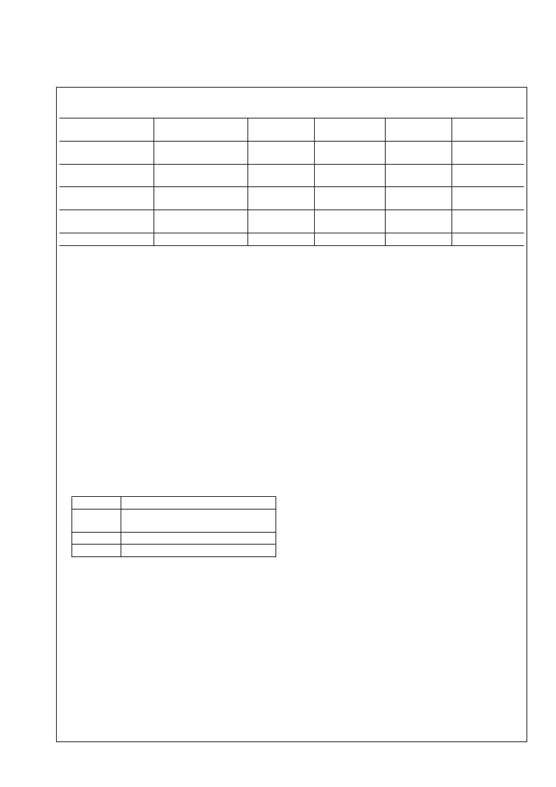
TABLE 11. Audio Path Configuration
Audio setting
Interface
Format
AAI Bit Clock
AAI Frame Clock
AAI Frame Sync
Pulse Length
14 Bits
OKI
MSM7717
OKI
MSM7717
Winbond
W681310
Winbond
W681360
PCM slave
(Note 24)
Advanced audio interface
8-bit log PCM
(a-law only)
8-bit log PCM
(a-law only)
8-bit log PCM
A-law and u-law
13-bit linear
480 kHz
8 kHz
Advanced audio interface
520 kHz
8 kHz
14 Bits
Advanced audio interface
520 kHz
8 kHz
14 Bits
Advanced audio interface
520 kHz
8 kHz
13 Bits
Advanced audio interface
8/16 bits
128 - 1024 kHz
8 kHz
8/16 Bits
Note 24:
In PCM slave mode, parameters are stored in NVS. Bit clock and frame clock must be generated by the host interface.
PCM slave configuration example:
PCM slave uses the slot
0, 1 slot per frame, 16 bit linear mode, long frame sync, normal
frame sync. In this case, 0x03E0 should be stored in NVS.
See “LMX9838 Software Users Guide” for more details.
11.4 AUXILIARY PORTS
11.4.1 RESET#
The RESET# is active low and will put radio and baseband
into reset.
11.4.2 General Purpose I/Os
The LMX9838 offers 3 pins which either can be used as indi-
cation and configuration pins or can be used for General
Purpose functionality. The selection is made out of settings
derived out of the power up sequence.
In General Purpose configuration the pins are controlled hard-
ware specific commands giving the ability to set the direction,
set them to high or low or enable a weak pull-up.
In alternate function the pins have pre-defined indication func-
tionality. Please see
Table 12
for a description on the alter-
nate indication functionality.
TABLE 12. Alternate GPIO Pin Configuration
Pin
OP4/PG4
Operation Mode pin to configure
Transport Layer settings during boot-up
PG6
GPIO - Link Status indication
PG7
RF Traffic indication
Description
12.0 Digital Smart Radio
12.1 FUNCTIONAL DESCRIPTION
The integrated Digital Smart Radio utilizes a heterodyne re-
ceiver architecture with a low intermediate frequency (2 MHz)
such that the intermediate frequency filters can be integrated
on chip. The receiver consists of a low-noise amplifier (LNA)
followed by two mixers. The intermediate frequency signal
processing blocks consist of a poly-phase bandpass filter
(BPF), two hard-limiters (LIM), a frequency discriminator
(DET), and a post-detection filter (PDF). The received signal
level is detected by a received signal strength indicator
(RSSI).
The received frequency equals the local oscillator frequency
(fLO) plus the intermediate frequency (fIF):
fRF = fLO + fIF (supradyne).
The radio includes a synthesizer consisting of a phase de-
tector, a charge pump, an (off-chip) loop-filter, an RF-fre-
quency divider, and a voltage controlled oscillator (VCO).
The transmitter utilizes IQ-modulation with bit-stream data
that is gaussian filtered. Other blocks included in the trans-
mitter are a VCO buffer and a power amplifier (PA).
12.2 RECEIVER FRONT-END
The receiver front-end consists of a low-noise amplifier (LNA)
followed by two mixers and two low-pass filters for the I- and
Q-channels.
The intermediate frequency (IF) part of the receiver front-end
consists of two IF amplifiers that receive input signals from
the mixers, delivering balanced I- and Q-signals to the poly-
phase bandpass filter. The poly-phase bandpass filter is di-
rectly followed by two hard-limiters that together generate an
AD-converted RSSI signal.
12.2.1 Poly-Phase Bandpass Filter
The purpose of the IF bandpass filter is to reject noise and
spurious (mainly adjacent channel) interference that would
otherwise enter the hard limiting stage. In addition, it takes
care of the image rejection.
The bandpass filter uses both the I- and Q-signals from the
mixers. The out-of-band suppression should be higher than
40 dB (f<1 MHz, f>3 MHz). The bandpass filter is tuned over
process spread and temperature variations by the autotuner
circuitry. A 5th order Butterworth filter is used.
12.2.2 Hard-Limiter and RSSI
The I- and Q-outputs of the bandpass filter are each followed
by a hard-limiter. The hard-limiter has its own reference cur-
rent. The RSSI (Received Signal Strength Indicator) mea-
sures the level of the RF input signal.
The RSSI is generated by piece-wise linear approximation of
the level of the RF signal. The RSSI has a mV/dB scale, and
an analog-to-digital converter for processing by the baseband
circuit. The input RF power is converted to a 5-bit value. The
RSSI value is then proportional to the input power (in dBm).
The digital output from the ADC is sampled on the BPKTCTL
signal low-to-high transition.
www.national.com
10
L
相關(guān)PDF資料 |
PDF描述 |
|---|---|
| LNBEH21 | LNB SUPPLY AND CONTROL IC WITH STEP-UP CONVERTER AND IC INTERFACE |
| LNBEH21PD | LNB SUPPLY AND CONTROL IC WITH STEP-UP CONVERTER AND IC INTERFACE |
| LNBEH21PD-TR | LNB SUPPLY AND CONTROL IC WITH STEP-UP CONVERTER AND IC INTERFACE |
| LNBK10 | LNB Supply And Control Voltage Regulator (Parallel Interface)(LNB 電源及控制電壓穩(wěn)壓器(并行接口)) |
| LP2950L-XX-T92-K | 100 mA LOW-DROPOUT VOLTAGE REGULATOR |
相關(guān)代理商/技術(shù)參數(shù) |
參數(shù)描述 |
|---|---|
| LMX9838SBX/NOPB | 功能描述:藍(lán)牙/802.15.1 模塊 RoHS:否 制造商:Murata Wireless Solutions 類:1 頻帶:2402 MHz to 2480 MHz 靈敏度:- 92 dBm 數(shù)據(jù)速率: 工作電源電壓:2.2 V to 3.3 V 輸出功率: 接口類型:PCM, UART 天線連接器類型:Chip 最大工作溫度:+ 85 C 尺寸:17.5 mm x 16 mm x 2 mm |
| LMXA301 | 制造商:Maglite 功能描述:3 Cell Lamp 制造商:MAG 功能描述:MAG 3 CELL LAMP, FOR USE WITH: MAG D CELL FLASHLIGHT 29-2000, MAG D CELL FLASHLIGHT 29-2010 制造商:Magnecraft 功能描述:MAGLITE LMXA301 LAMPS 3 CELL |
| LMXA301L | 制造商:MAG-LITE 功能描述: |
| LMXA401 | 制造商:Maglite 功能描述:4 Cell Lamp 制造商:MAG 功能描述:MAGLITE LMXA401 LAMPS 4 CELL 制造商:MAG 功能描述:MAG 4 CELL LAMP, FOR USE WITH: MAG D CELL FLASHLIGHT 29-2015, MAG D CELL FLASHLIGHT 29-2020 |
| LMXA401L | 制造商:MAG-LITE 功能描述: |
發(fā)布緊急采購(gòu),3分鐘左右您將得到回復(fù)。